Quantum-confinement stark effect optical modulator
a quantum-confinement, stark-effect technology, applied in the field of quantum-confinement stark-effect optical modulators, can solve the problems of degrading device characteristics, difficult to adopt a selective growth technique, scattering loss of transmitted light,
- Summary
- Abstract
- Description
- Claims
- Application Information
AI Technical Summary
Benefits of technology
Problems solved by technology
Method used
Image


Examples
first embodiment
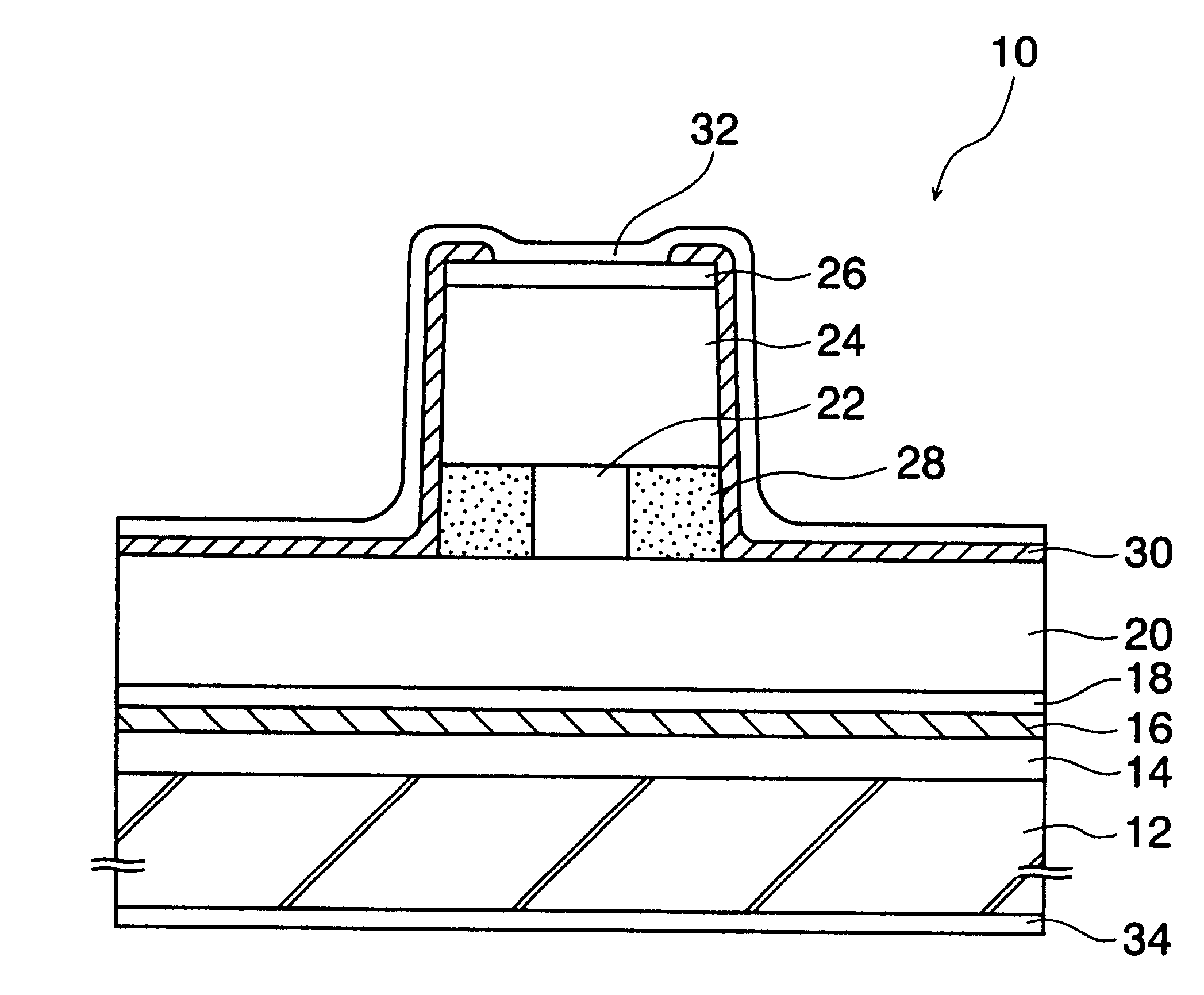
Referring to FIG. 2, an optical modulator, generally designated by numeral 10, is an example of the first aspect of the present invention. The optical modulator 10 includes an n-InP substrate 12, and an AlGaInAs-based layer structure including an n-InP cladding layer 14, an AlGaInAs-based MQW 16, a GaInAsP optical confinement layer a p-InP cladding layer 20, a p-AlInAs layer 22, a p-InP cladding layer 24 and a p-GaInAs contact layer 26, which are consecutively grown on the n-InP substrate 12.
The n-InP cladding layer 14 is 100 nm thick, and has a carrier density of 5.times.10.sup.17 cm.sup.-3 : the MQW has a lasing wavelength ( .lambda. g) of 1.52 .mu.m: the GaInAsP optical confinement layer 18 is 10 nm thick and has a wavelength of 1.2 .mu.m: the p-InP cladding layer 20 is 150 nm thick and has a carrier density of 5.times.10.sup.17 cm.sup.-3 : the p-AlInAs layer 22 is 100 nm thick and has a carrier density of 1.times.10.sup.18 cm.sup.-3 : the p-InP cladding layer 24 is 2000 nm thick...
second embodiment
Fabrication of Second Embodiment
Referring to FIGS. 7A to 7H, there are shown fabrication steps for manufacturing the optical device of the second embodiment.
In FIG. 7A, a layer structure for the GaInAsP-based based DFB-LD 40 is formed over the entire surface of an n-Inp substrate 12 by using known processes. More specifically, a 100-nm-thick n-InP cladding layer 44 having a carrier density of 5.times.10.sup.17 cm.sup.-3 a GaInAsP-based MQW 46 having a lasing wavelength of 1.55 .mu.m and a 10-nm-thick GaInAsP waveguide layer 48 are grown on the n-InP substrate 12 by using an epitaxial technique. Then, a diffraction grating is formed in the GaInAsP layer 48 by a known technique, followed by epitaxially growing thereon a 200-nm-thick p-InP cladding layer 50.
Subsequently, a SiN film is formed on the entire surface including the optical modulator area (which is herein designated also by numeral 10) and the DFB-LD area (which is herein designated also by numeral 40), followed by patternin...
third embodiment
Referring to FIG. 8, a semiconductor optical device according to the third embodiment includes a semiconductor laser device 70 and an optical modulator 100 which are coupled by a coupling area 71, similarly to the second embodiment. In this embodiment, the layers in the semiconductor laser device 70 and the optical modulator 100 have different film compositions as viewed in the thickness direction as a result of the area-selective growth process. The layer compositions in the semiconductor laser device 70 is similar to those in the optical modulator 100. FIGS. 9 and 10 show the semiconductor laser device 70 and the optical modulator 10, respectively.
The semiconductor laser device 70 is a DFB-LD of ridge waveguide type, and has an AlGaInAs-based layer structure including an n-InP cladding layer 74, an AlGaInAs-based MQW 76, a GaInAsP layer 78 including a diffraction grating, a p-InP cladding layer 80, a p-InP cladding layer 81, a p-AlInAs layer 82, a p-InP cladding layer 84 and a p-G...
PUM
| Property | Measurement | Unit |
|---|---|---|
| width | aaaaa | aaaaa |
| electric field | aaaaa | aaaaa |
| length | aaaaa | aaaaa |
Abstract
Description
Claims
Application Information
 - R&D
- Intellectual Property
- Life Sciences
- Materials
- Tech Scout
- Unparalleled Data Quality
- Higher Quality Content
- 60% Fewer Hallucinations
Browse by: Latest US Patents, China's latest patents, Technical Efficacy Thesaurus, Application Domain, Technology Topic, Popular Technical Reports.
© 2025 PatSnap. All rights reserved.Legal|Privacy policy|Modern Slavery Act Transparency Statement|Sitemap|About US| Contact US: help@patsnap.com