
Determining verification coverage using circuit properties

a verification coverage and circuit technology, applied in the direction of cad circuit design, program control, instruments, etc., can solve the problems of increasing manufacturing costs, requiring a long time to write a sufficient set of test vectors, and a large number of test vectors

Inactive Publication Date: 2003-07-15
AVERANT
View PDF2 Cites 31 Cited by
  • Summary
  • Abstract
  • Description
  • Claims
  • Application Information

AI Technical Summary

Benefits of technology

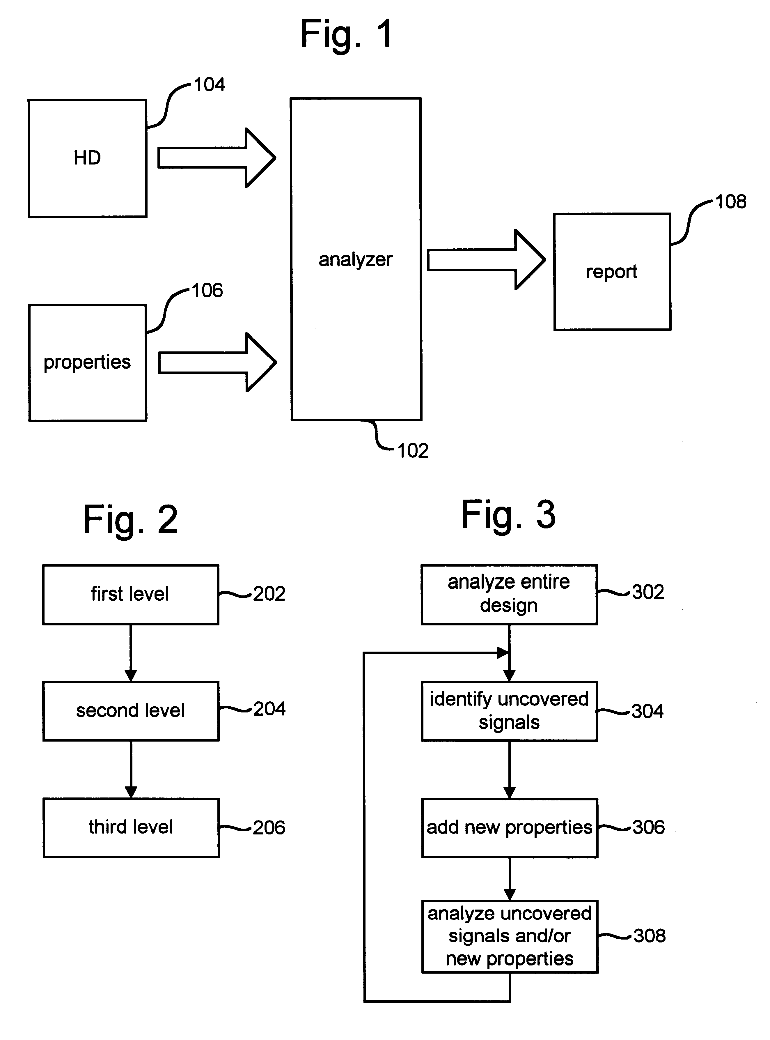
Analyzer 102 can perform any one of three levels of analysis so users can make faster progress in verifying a design than with a single level approach. Level 1 is extremely fast. Level 2 is more accurate than Level 1, but slower than level 1. Level 3 is more accurate than levels 1 and 2, and is performed slower than levels 1 and 2. One embodiment of the present invention can perform all three levels. Other embodiments of the present invention will only perform one of the levels or two of the levels.

Problems solved by technology

As circuit designs become more complex, the cost of manufacturing increases and the time-to-market becomes even more critical, it has become apparent that circuit designers must verify their designs prior to manufacturing.
It typically takes a long time to write a sufficient set of test vectors and rarely do these test vectors provide one hundred percent coverage.
Another drawback of using test vectors is that the time needed to run the simulation using the test vectors can be extremely long, even to the point where the design process becomes unreasonably stalled.
Because time to market is critical and engineering resources are expensive, the prior solution for providing verification of a design is not sufficient.
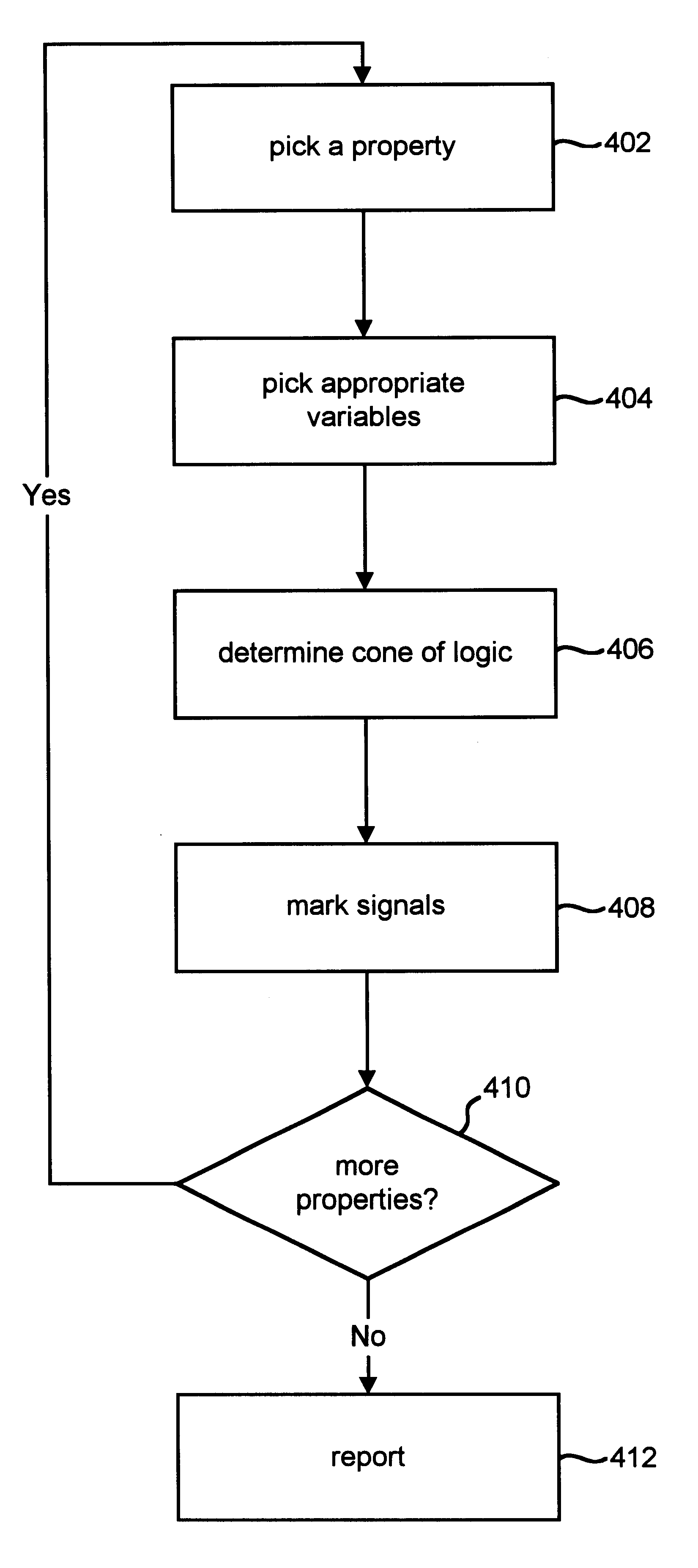
In other words, a counter which doesn't satisfy this property doesn't work properly as expected.

Method used


Image

  • Determining verification coverage using circuit properties
  • Determining verification coverage using circuit properties
  • Determining verification coverage using circuit properties

Examples


Embodiment Construction

has been presented for purposes of illustration and description. It is not intended to be exhaustive or to limit the invention to the precise form disclosed, and obviously many modifications and variations are possible in light of the above teaching. The described embodiments were chosen in order to best explain the principles of the invention and its practical application to thereby enable others skilled in the art to best utilize the invention in various embodiments and with various modifications as are suited to the particular use contemplated. It is intended that the scope of the invention be defined by the claims appended hereto.


PUM


Abstract

A system is disclosed to provide static coverage analysis. The system receives at least two inputs including a hardware description and a set of properties. Using the methods of the present invention, the system determines what portions of the design can be verified using the set of properties. In one embodiment, the invention includes three levels of analysis. Each level provides a different tradeoff between level of accuracy and speed.

Description

1. Field of the InventionThe present invention is directed to system for determining the extent that a design has been or can be verified.2. Description of the Related ArtAs circuit designs become more complex, the cost of manufacturing increases and the time-to-market becomes even more critical, it has become apparent that circuit designers must verify their designs prior to manufacturing. That is, after a given circuit is designed, the circuit designer will perform tests or simulations using a computer to verify that the circuit design will operate as intended. For example, a circuit designer may use a schematic capture program to draw a circuit or may use a hardware description language to describe a circuit. The circuit designer will then create tests in order to simulate operation of the circuit.Even if a design passes the tests created by the designer, it does not mean that the circuit will operate as intended. There may be various modes of behavior which are not verified by t...

Claims


Application Information

Patent Timeline
IPC IPC(8): G01R31/28G01R31/3183G06F17/50
CPCG01R31/31835G01R31/318357G01R31/318364G06F17/5022G06F30/33
Inventor HOJATI, RAMIN
Owner AVERANT
Learn More