Semiconductor device and method of manufacturing same
a technology of semiconductor devices and semiconductors, applied in semiconductor devices, semiconductor/solid-state device details, electrical apparatus, etc., can solve the problems of reduced yield, increased process cost, and long ta
- Summary
- Abstract
- Description
- Claims
- Application Information
AI Technical Summary
Problems solved by technology
Method used
Image

Examples
first embodiment
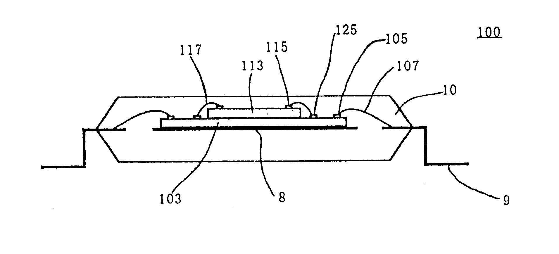
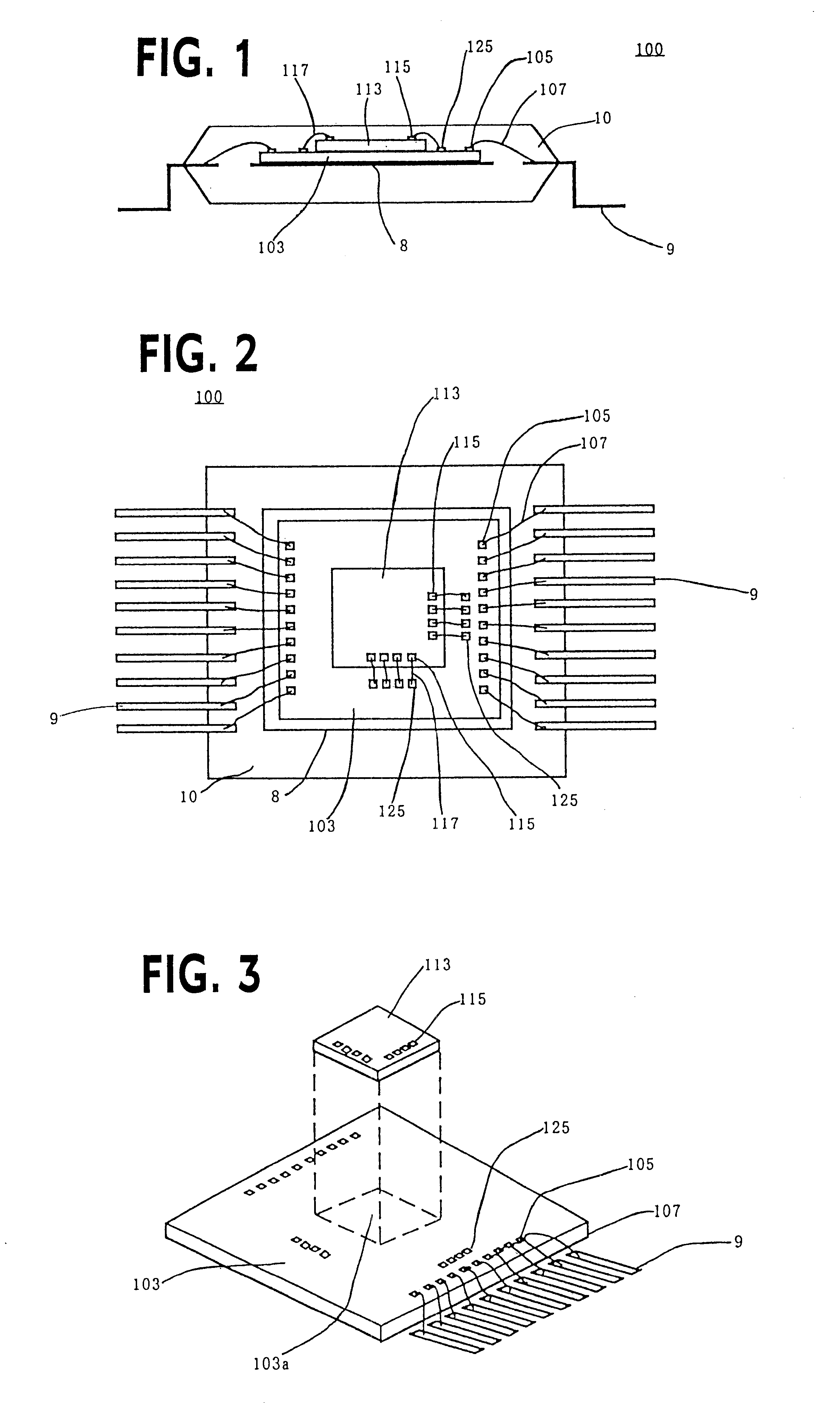
Semiconductor devices of the present invention will hereinafter be described in detail with reference to the accompanying drawings. FIG. 1 is a cross-sectional view showing an internal structure of an MCP type semiconductor device 100 according to the present invention, and FIG. 2 is a plan view illustrating the internal structure of the semiconductor device 100, respectively. In FIG. 1, the same elements of structure as those shown in FIGS. 16 through 18 are identified by the same reference numerals.
In FIGS. 1 and 2, the semiconductor device 100 has an LSI chip 103 which serves as a first semiconductor element, and an LSI chip 113 which serves as a second semiconductor element. The LSI chip 103 and the LSI chip 113 are both similar in shape to each other (rectangular in the present invention).
The LSI chip 103 is fixed and placed on a substantially central area of a die 8 with an adhesive provided between the reverse side or back of the LSI chip 103 and the die 8. A plurality of fir...
second embodiment
A second embodiment provides one to which the semiconductor device according to the first embodiment of the present invention is applied, and which is improved so as to solve the above-described problems which arise between the EEPROM version micon and the mask ROM version micon. A semiconductor device according to the present invention will be described below with reference to the drawings. FIGS. 5 and 6 are respectively plan views of the semiconductor device according to the second embodiment of the present invention. FIG. 5 is a view showing the semiconductor device used as an EEPROM version micon, and FIG. 6 is a view showing the semiconductor device used as a mask ROM version micon, respectively. FIGS. 5 and 6 correspond to FIG. 2. The same elements of structure as those shown in FIG. 2 are identified by the same reference numerals.
In FIG. 5, an EEPROM defined as a program memory is placed over an LSI chip 213. An LSI chip 203 having a main surface on which the LSI chip 213 is ...
PUM
 Abstract
Description
Claims
Application Information
 - R&D
- Intellectual Property
- Life Sciences
- Materials
- Tech Scout
- Unparalleled Data Quality
- Higher Quality Content
- 60% Fewer Hallucinations
Browse by: Latest US Patents, China's latest patents, Technical Efficacy Thesaurus, Application Domain, Technology Topic, Popular Technical Reports.
© 2025 PatSnap. All rights reserved.Legal|Privacy policy|Modern Slavery Act Transparency Statement|Sitemap|About US| Contact US: help@patsnap.com