
Integrated circuit device

a circuit device and integrated circuit technology, applied in the direction of basic electric elements, electrical apparatus construction details, support structure mounting, etc., can solve the problems of poor or uneven sensitivity, further increase the overall thickness, hamper the reduction of cost and weight,

Inactive Publication Date: 2002-12-03
ROHM CO LTD
View PDF4 Cites 99 Cited by
  • Summary
  • Abstract
  • Description
  • Claims
  • Application Information

AI Technical Summary

Benefits of technology

Another object of the present invention is to provide an integrated circuit device having IC chips forming a chip-on-chip structure that reduces the amount of shielding material required, or even eliminates the need therefor, in providing necessary shielding and thereby helps achieve cost reduction and weight reduction.
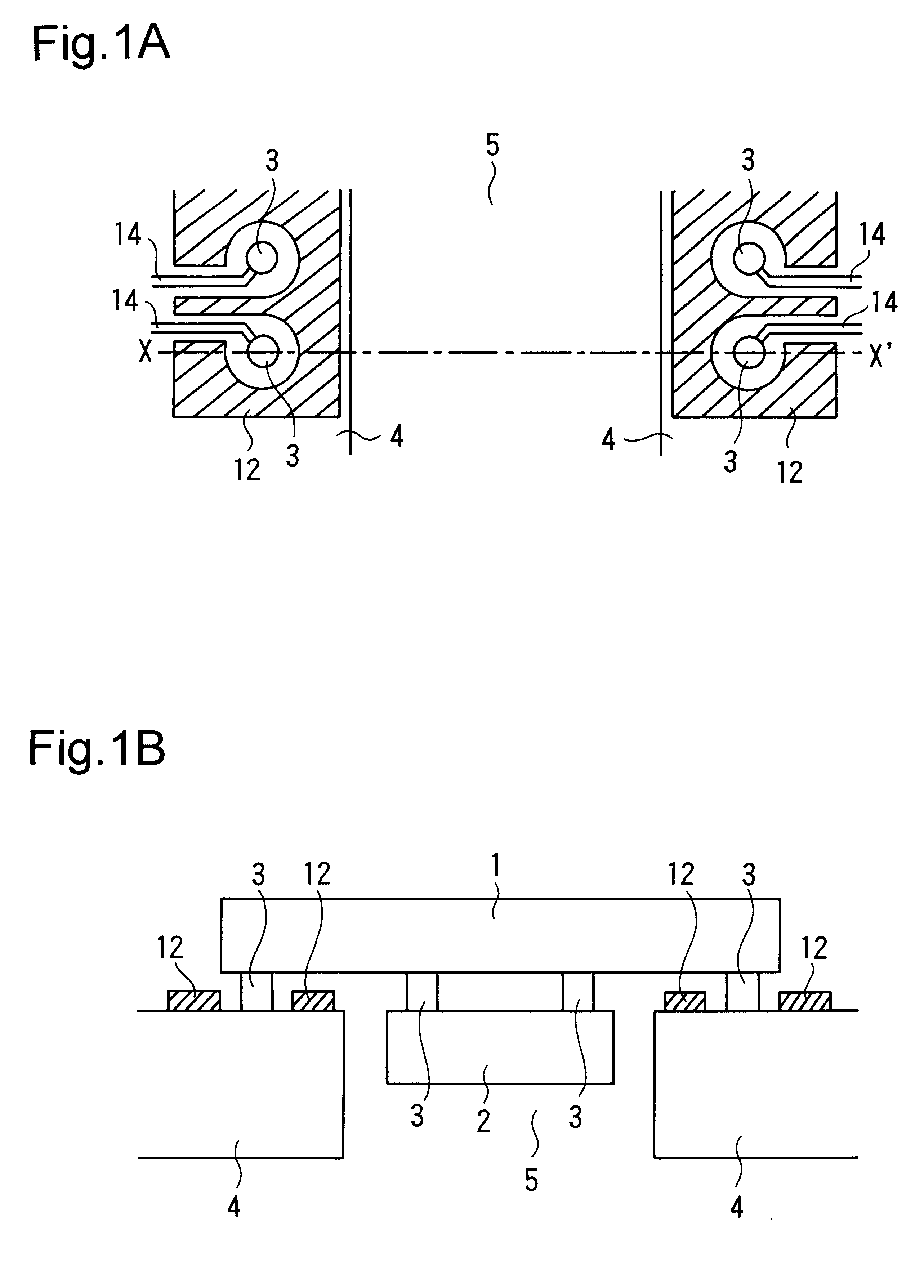
In this arrangement, one of the IC chips forming a chip-on-chip structure is accommodated in the hole formed in the circuit board. This helps achieve further thickness reduction. In addition, the obverse surfaces of the IC chips (i.e. the surfaces on which the IC chips are bonded together) are located closer to the circuit board. This makes it possible to mount the IC chips, even though they form a chip-on-chip structure, on the circuit board on a wireless basis (without using wires), i.e. through connection using bumps or by another means. In this way, it is possible to reduce trouble due to inductance in a circuit that handles a high-frequency signal.
The circuit board may have shielding pattern formed around the portion thereof where the first IC chip is connected to the circuit board. This makes it possible to shield the noise coming from where the IC chip is connected to the circuit board, and thus helps enhance the shielding effect.
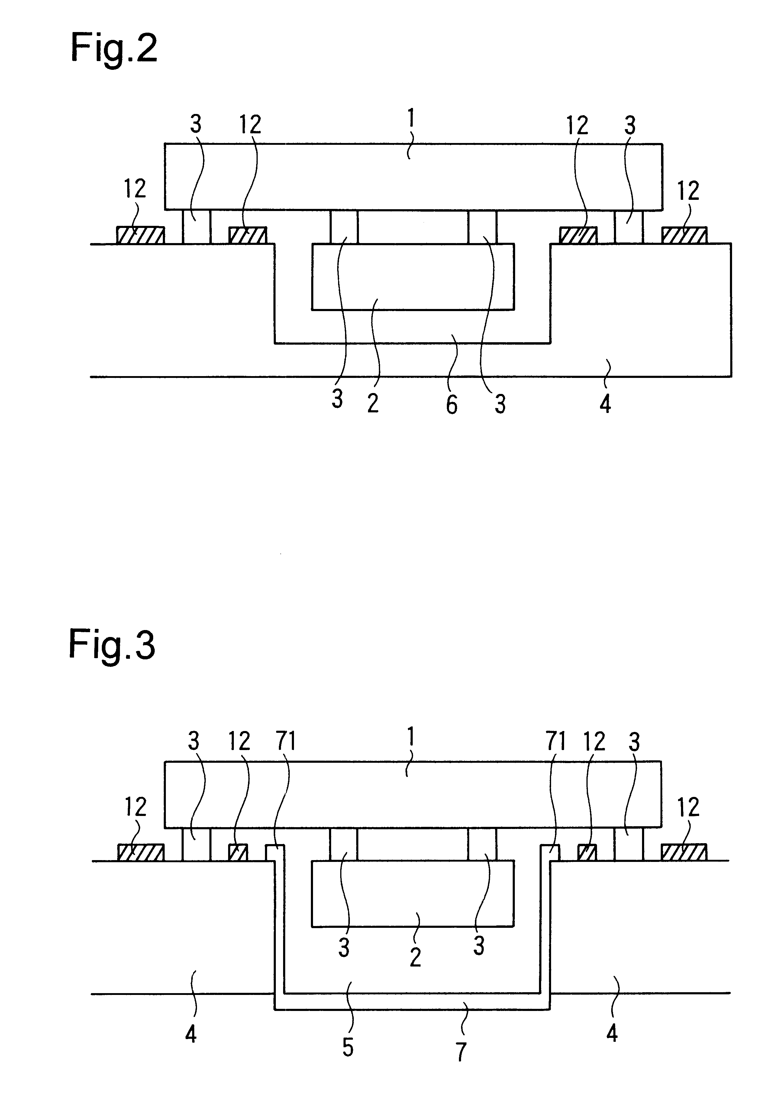
Shielding material connected to fixed potential point may be provided in the hole formed in the circuit board. This permits the portion of the circuit board on which the IC chips forming a chip-on-chip structure are mounted to be surrounded by the shielding material connected to the fixed potential point and by the reverse surfaces of the IC chips (the surfaces of the IC chips opposite to the surfaces thereof on which they are bonded together), which also offer a shielding effect. Thus, it is possible to obtain a sufficient shielding effect.
The shielding material has only to be somewhat larger than the smaller of the IC chips forming a chip-on-chip structure. This helps reduce the amount of shielding material required as compared with conventional arrangements and thereby achieve cost reduction and eight reduction. By making the shielding material somewhat larger than the larger of the IC chips forming a chip-on-chip structure, it is possible to obtain a higher shielding effect.
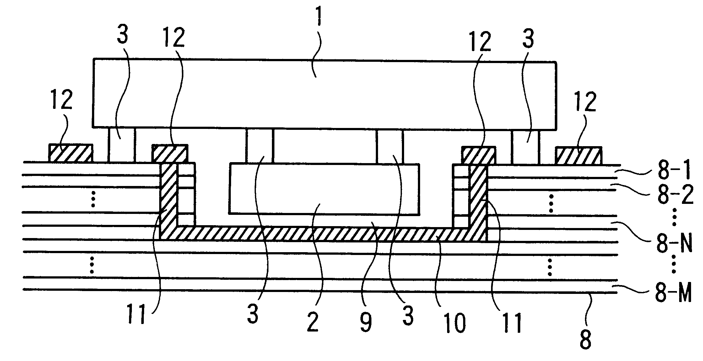
In this arrangement, one of the IC chips forming a chip-on-chip structure is accommodated in the recess formed in the multilayer circuit board. This helps achieve further thickness reduction. In addition, the portion of the multilayer circuit board on which the IC chips forming a chip-on-chip structure are mounted is surrounded by the wiring pattern connected to the fixed potential point and formed inside the multilayer circuit board and by the reverse surfaces of the IC chips (the surfaces of the IC chips opposite to the surfaces thereof on which they are bonded together), which also offer a shielding effect. Thus, it is possible to obtain a sufficient shielding effect. Since the wiring pattern formed inside the multilayer circuit board is used as shielding material, there is no need to provide shielding material separately, and thus it is possible to achieve further cost reduction and weight reduction.

Problems solved by technology

As a result, in particular in the case of a circuit that handles a high-frequency signal, the inductance of the wires 400 tend to cause poor or uneven sensitivity.
Providing shielding in this way, however, not only requires a large amount of shielding material, and thus hampers cost reduction and weight reduction, but also further increases the overall thickness.
This often makes an arrangement like this unusable in thin devices such as IC cards and cellular telephones.

Method used


Image

  • Integrated circuit device
  • Integrated circuit device
  • Integrated circuit device

Examples


first embodiment

Hereinafter, embodiments of the present invention will be described with reference to the drawings. FIG. 1A is a top view of the circuit board (in its state before IC chips are mounted thereon) of the integrated circuit device of the invention. FIG. 1B is a sectional view taken along line X-X' shown in FIG. 1A.

In the first embodiment, a chip-on-chip structure is formed by electrically connecting together a first IC chip 1 and second IC chip 2 through bumps 3 such as gold bumps. Wiring patterns 14 are aid so as to originate respectively from bumps 3 formed on a circuit board 4. The circuit board 4 is made of resin, ceramics, or the like, and has a through hole formed therein so as to be large enough to accommodate the second IC chip 2, i.e. the smaller of the two IC chips, therein.

The first IC chip 1 is so positioned that the second IC chip 2 is accommodated in the through hole 5 formed in the circuit board 4, and is electrically connected to the wiring pattern 14 formed on the circu...

second embodiment

In this second embodiment, the portion of the circuit board on which the first and second IC chips 1 and 2 are mounted is surrounded by the shielding material 7 connected to the fixed potential point and by the reverse surface of the first IC chip 1 (the surface of the first IC chip 1 opposite to the surface thereof to which the second IC chip 2 is bonded), which also offers a shielding effect. Thus, it is possible to obtain a sufficient shielding effect.

Moreover, the shielding material 7 has only to be at least somewhat larger than the second IC chip 2, i.e. the smaller of the two IC chips, up to about the size of the first IC chip 1. This helps reduce the amount of shielding material required and thereby achieve cost reduction and weight reduction. By making the shielding material 7 somewhat larger than the first IC chip 1 as shown in FIG. 5, it is possible to expect a higher shielding effect.

FIG. 6 is a sectional view of the integrated circuit device of a third embodiment of the ...

third embodiment

In this third embodiment, the portion of the circuit board on which the first and second IC chips 1 and 2 are mounted is surrounded by the wiring pattern 10 and the via conductors 11 connected to the fixed potential point and by the reverse surface of the first IC chip 1 the surface of the first IC chip 1 opposite to the surface thereof to which the second IC chip 2 is bonded), which also offers a shielding effect. Thus, it is possible to obtain a sufficient shielding effect. Moreover, a wiring pattern formed in the multilayer circuit board 8 is used as shielding material, and therefore there is no need to provide shielding material separately. This makes it possible to achieve further cost reduction and weight reduction.


PUM


Abstract

An integrated circuit device as a first IC chip, a second IC chip, and a circuit board having a hole formed therein that is large enough to permit the second IC chip to be accommodated therein. The first and second IC chips are bonded together so as to be electrically connected together, and the first IC chip is mounted on the circuit board with the second IC chip accommodated in the hole formed in the circuit board. Here, one of the IC chips forming a chip-on-chip structure is accommodated in the hole formed in the circuit board, making further thickness reduction possible. Moreover, the obverse surfaces of the IC chips are located closer to the circuit board, making possible wireless mounting of the IC chips, despite forming a chip-on-chip structure, on the circuit board through connection using bumps. This helps reduce trouble due to inductance in a circuit that handles a high-frequency signal.

Description

1. Field of the InventionThe present invention relates to an integrated circuit device having IC chips forming a so-called chip-on-chip structure, in which two IC chips are bonded together through bumps or by another means so as to be electrically connected together.2. Description of the Prior ArtConventionally, when two semiconductor chips are mounted on a circuit board, they are sometimes bonded together through bumps or by another means so as to be electrically connected together (hereinafter referred to as a "chip-on-chip structure"). As compared with mounting two chips separately, adopting a chip-on-chip structure offers the advantage of making of the area required on a circuit board smaller.However, conventionally, as shown in FIG. 7, IC chips 100 and 200 forming a chip-on-chip structure are usually simply placed on a circuit board 300, and thus tend to increase the overall thickness. Moreover, the obverse surface of the IC chip 100 (i.e. that surface of the IC chip 100 to whi...

Claims


Application Information

Patent Timeline
IPC IPC(8): H01L23/12H01L25/065H01L23/552H01L23/13H01L23/02H01L25/07H01L25/18
CPCH01L23/13H01L23/552H01L25/0657H01L2224/16145H01L2224/48091H01L2224/48464H01L2225/06513H01L2225/06517H01L2225/06527H01L2924/01013H01L2924/01029H01L2924/01079H01L2924/14H01L2924/15153H01L2924/1517H01L2924/16152H01L2924/30107H01L2924/3025H01L2924/00014H01L24/48H01L2224/45144H01L24/45H01L2224/0401H01L2224/45015H01L2924/207
Inventor SHIMADA, YOSHIKAZUMOCHIDA, HIROO
Owner ROHM CO LTD
Learn More