
Method for cleaning inside of chamber using RF plasma

a technology of radio frequency plasma and cleaning chamber, which is applied in the direction of plasma technique, cleaning of hollow articles, coatings, etc., can solve the problems of contaminating the wafer, contaminating the reaction product or by products, and accumulating all the contaminating products

Inactive Publication Date: 2001-10-23
SAMSUNG ELECTRONICS CO LTD
View PDF3 Cites 28 Cited by
  • Summary
  • Abstract
  • Description
  • Claims
  • Application Information

AI Technical Summary

Benefits of technology

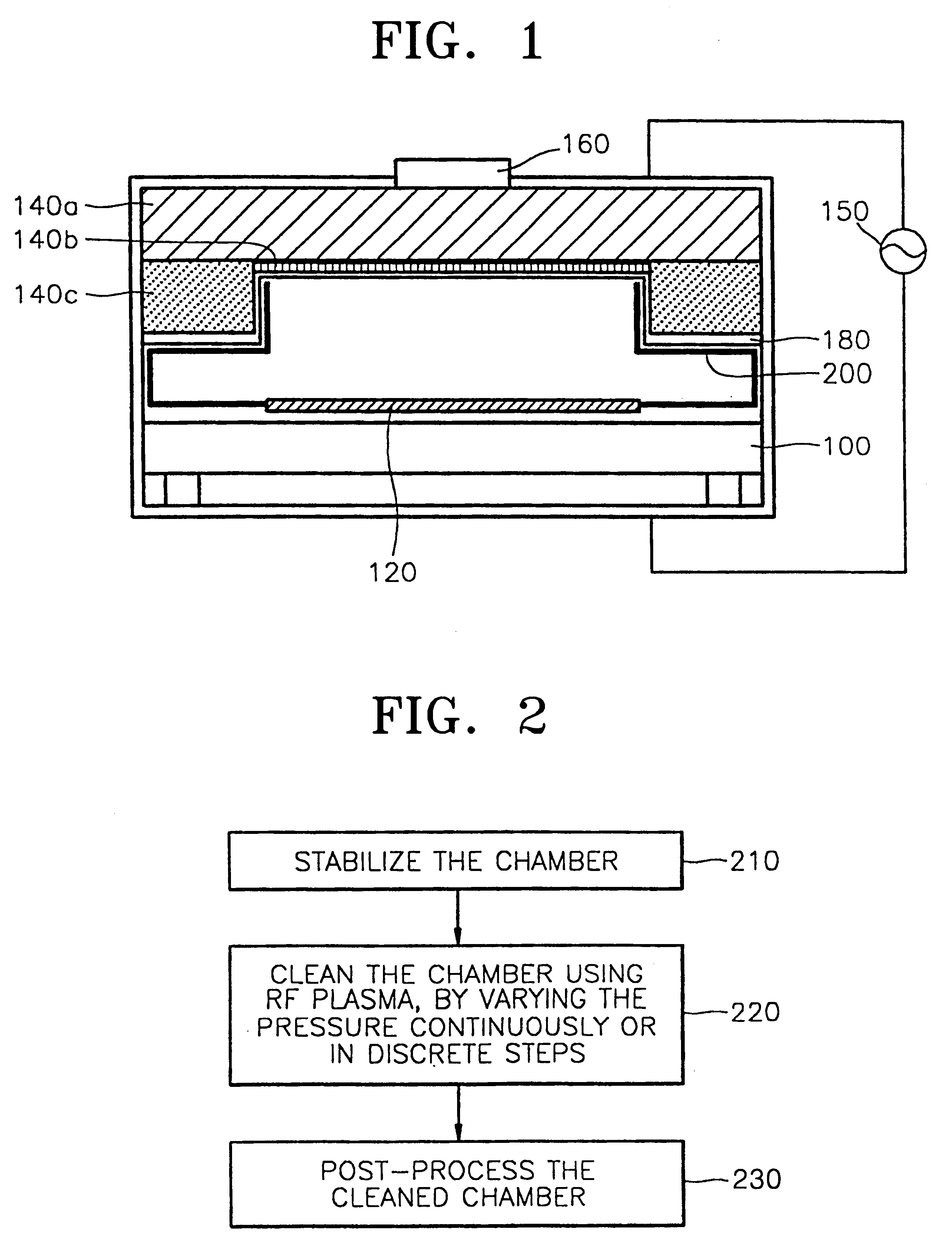
It is therefore an aspect of the present invention to provided a method for cleaning the inside of a chamber using a radio frequency (RF) plasma, that includes stabilizing the inside of the chamber so that the inner surface coated with accumulated layers of contaminants can be removed through cleaning. The inside of the chamber is then cleaned using the RF plasma while continuously varying the pressure inside the chamber.
In another aspect of the invention, the RF plasma is obtained by applying RF power that varies according to pressure changes in the chamber, which ranges from 150 W to 500 W. It is an advantage of the present invention that the cleaning step may be performed for less than 200 seconds.
It is an advantage of the present invention that by varying pressure and RF power inside the chamber, all parts inside the chamber are cleaned.

Problems solved by technology

However, when using CVD, a film of unwanted, contaminating reaction products or by products is deposited all over the inside of the chamber, and more importantly, on the surface of the wafer itself.
These contaminants affect the physical and chemical properties of the film deposited on the wafer, and generate particles which further contaminate the wafer.
However, only certain parts of the chamber are cleaned, permitting contaminating reaction products to accumulate on other parts of the chamber over many deposition and cleaning cycles.
Also, since adhesion between the accumulated deposited materials is weak, over time the deposited materials separate from or fall off of the surface of the chamber generating particles that reduce semiconductor device yield.
However, frequent cleaning reduces throughput and is inefficient.
If the applied pressure is out of this range, that is, less than 100 m Torr or higher than 800 m Torr, the chamber and the equipment inside may be damaged.

Method used


Image

  • Method for cleaning inside of chamber using RF plasma
  • Method for cleaning inside of chamber using RF plasma
  • Method for cleaning inside of chamber using RF plasma

Examples


second embodiment

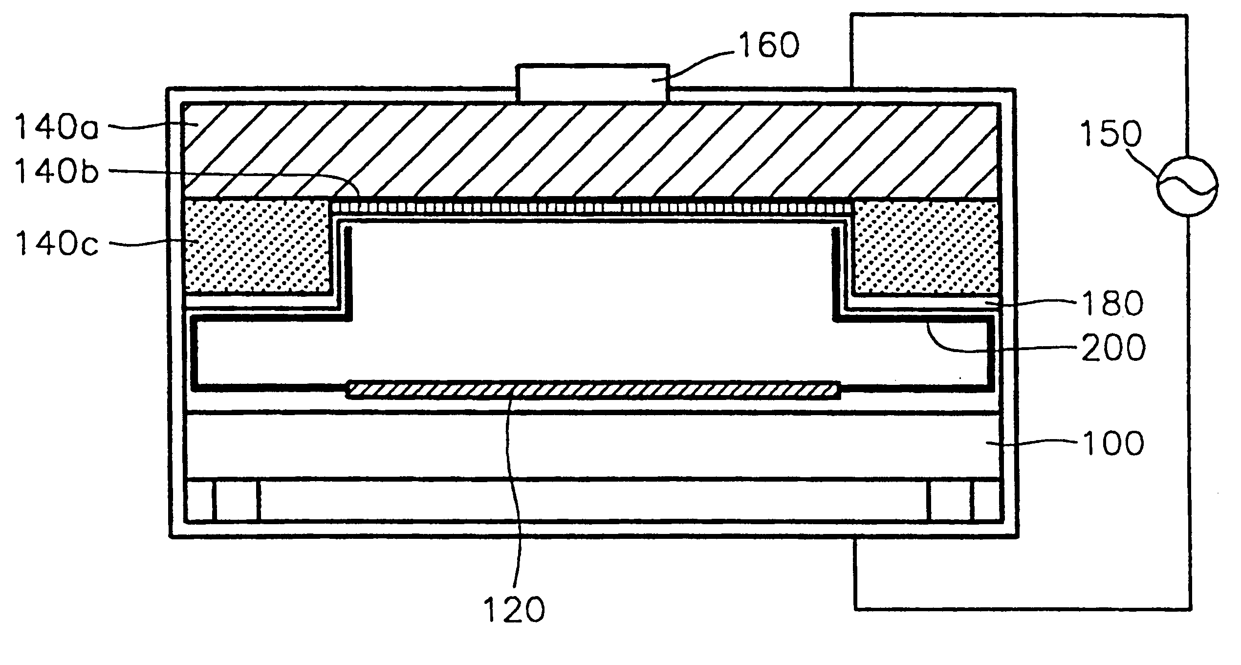
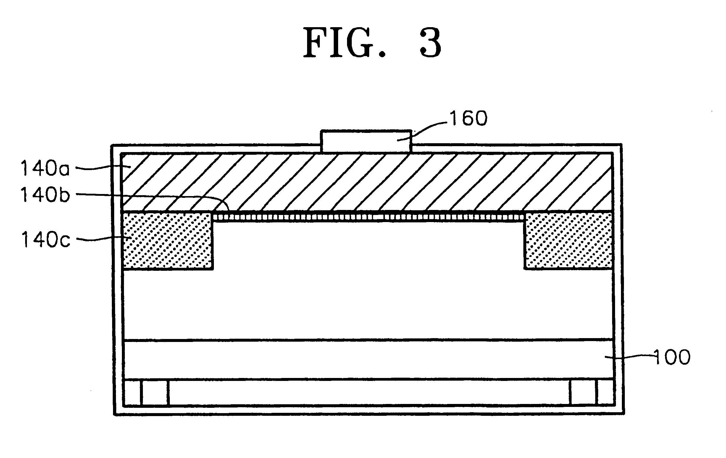
The cleaning was then performed using RF plasma. In this example, the pressure of the chamber was varied to three different levels during the cleaning, as in the present invention. First, the pressure of the chamber was maintained at 600 m Torr, nitrogen trifluoride (NF.sub.3) was introduced into the chamber via the gas inlet 160 at a rate of 250 sccm for 120 seconds, and 350 W RF power was applied between the shower head 140a and the suscepter 100 to form an RF plasma in the chamber. The generated RF plasma reacted with the tungsten silicide layers 200 and 180 (see FIG. 1) deposited on the inner surface of the chamber. The backside Ar gas was continuously introduced at a rate of 30 sccm during the cleaning process in order to prevent nitrogen trifluoride (NF.sub.3) from flowing below the suscepter to remove the unnecessary layers formed below the suscepter through Ar sputtering.

Second, the pressure of the chamber was lowered to 400 m Torr, and nitrogen trifluoride (NF.sub.3) was in...


PUM

PropertyMeasurementUnit
Poweraaaaaaaaaa
Poweraaaaaaaaaa
Fractionaaaaaaaaaa

Abstract

A method for cleaning the inside of a chamber using a radio frequency (RF) plasma, in which all parts within the camber can be completely cleaned. In the cleaning method, the conditions inside the chamber are stabilized. Then, impurities are cleaned from the inside of the chamber using the RF plasma, while varying the pressure in the chamber continuously or in discrete steps.

Description

1. Field of the InventionThe present invention relates to a method for manufacturing a semiconductor device, and more particularly, to a method for cleaning the inside of a chamber using a radio frequency (RF) plasma.2. Description of the Related ArtIn order to form a film on the surface of a wafer when manufacturing a semiconductor device, a chemical vapor deposition (CVD) method based on a gaseous reaction within a vacuum chamber is used. However, when using CVD, a film of unwanted, contaminating reaction products or by products is deposited all over the inside of the chamber, and more importantly, on the surface of the wafer itself. These contaminants affect the physical and chemical properties of the film deposited on the wafer, and generate particles which further contaminate the wafer. It is therefore necessary to remove the unwanted reaction product deposited inside the chamber after a certain number of wafers have been processed. A cleaning method using a plasma has been use...

Claims


Application Information

Patent Timeline
IPC IPC(8): C23C16/44H01J37/32H01L21/02H01L21/285H05H1/46H01L21/302H01L21/304H01L21/3065
CPCC23C16/4405H01J37/32862H01L21/28518H01L21/28556Y10S438/905H01L21/304
Inventor JEON, JIN-HO
Owner SAMSUNG ELECTRONICS CO LTD
Learn More