
Demultiplexer for a molecular wire crossbar network (MWCN DEMUX)

a crossbar network and multi-layer technology, applied in the field of demultiplexers for two-dimensional arrays, can solve the problems of losing the size advantage of the molecular wire nano-architecture, and achieve the effect of no effective defect tolerance and easy destruction

Inactive Publication Date: 2001-07-03
HEWLETT-PACKARD ENTERPRISE DEV LP
View PDF13 Cites 746 Cited by
  • Summary
  • Abstract
  • Description
  • Claims
  • Application Information

AI Technical Summary

Benefits of technology

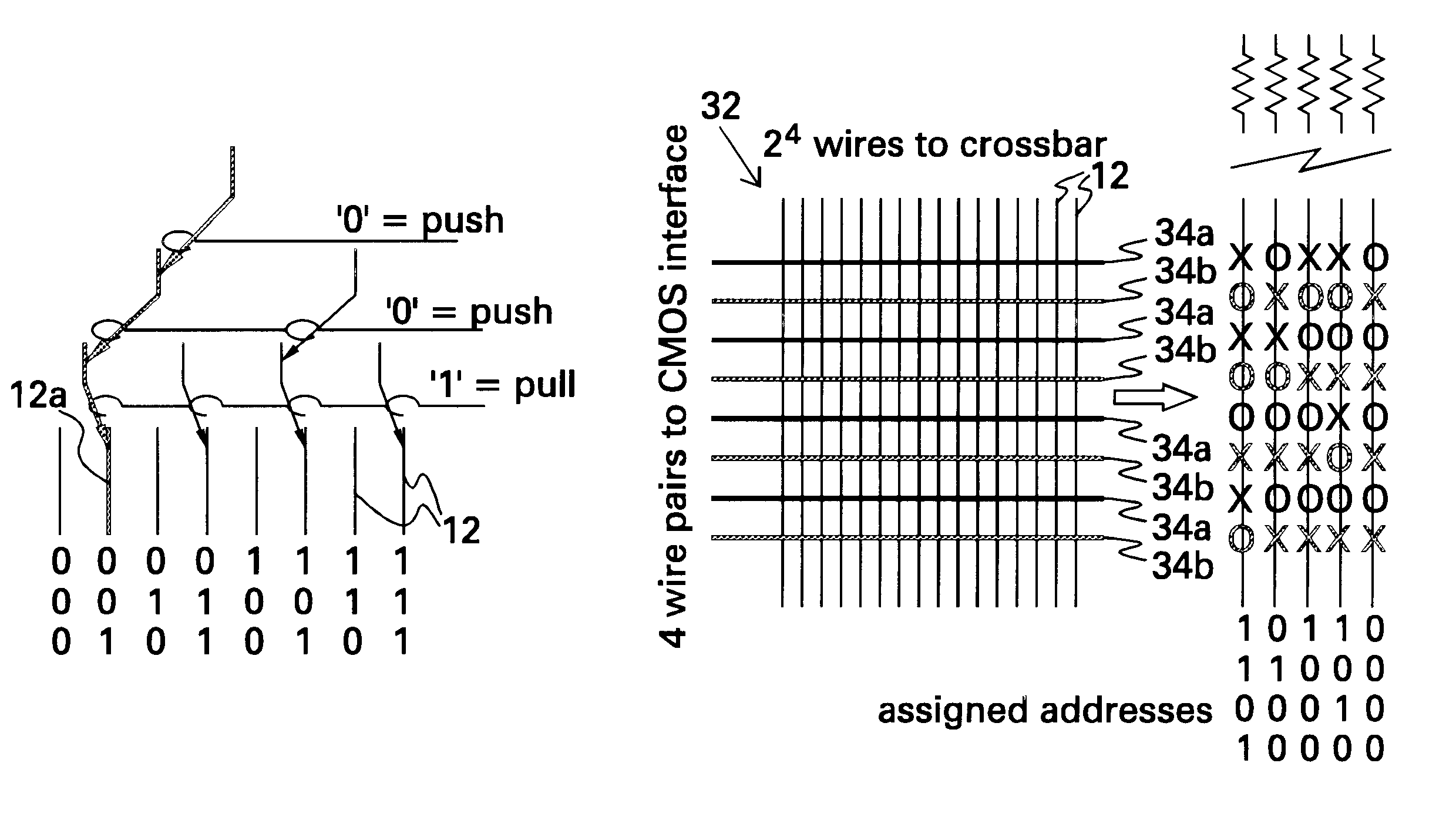
The present invention solves both the problems of data input and output to a molecular electronic system and also bridges the size gap between CMOS and molecules with an architecture that can scale up to extraordinarily large numbers of molecular devices. It is important that the architecture be able to scale to a very large number of components. If all of the nanometer sized wires must be spread out to the same pitch as the lithographically-formed components with which they communicate, then the size advantages of the molecular wire nano-architecture are going to be lost. If, however, the wires are assembled at the full density that the nanometer spacing would allow, then in the space accessible to a single lithographically-formed wire, close to a hundred distinct molecular wires must be connected. This invention solves this problem, by allowing selective connection to all of the molecular wires.

Problems solved by technology

If all of the nanometer sized wires must be spread out to the same pitch as the lithographically-formed components with which they communicate, then the size advantages of the molecular wire nano-architecture are going to be lost.

Method used


Image

  • Demultiplexer for a molecular wire crossbar network (MWCN DEMUX)
  • Demultiplexer for a molecular wire crossbar network (MWCN DEMUX)
  • Demultiplexer for a molecular wire crossbar network (MWCN DEMUX)

Examples


Embodiment Construction

Definitions

As used herein, the term "self-aligned" as applied to "junction" means that the junction that forms the switch and / or other electrical connection between two wires is created wherever two wires, either of which may be coated or functionalized, cross each other, because it is the act of crossing that creates the junction.

The term "self-assembled" as used herein refers to a system that naturally adopts some geometric pattern because of the identity of the components of the system; the system achieves at least a local minimum in its energy by adopting this configuration.

The term "singly configurable" means that a switch can change its state only once via an irreversible process such as an oxidation or reduction reaction; such a switch can be the basis of a programmable read only memory (PROM), for example.

The term "reconfigurable" means that a switch can change its state multiple times via a reversible process such as an oxidation or reduction; in other words, the switch can...


PUM


Abstract

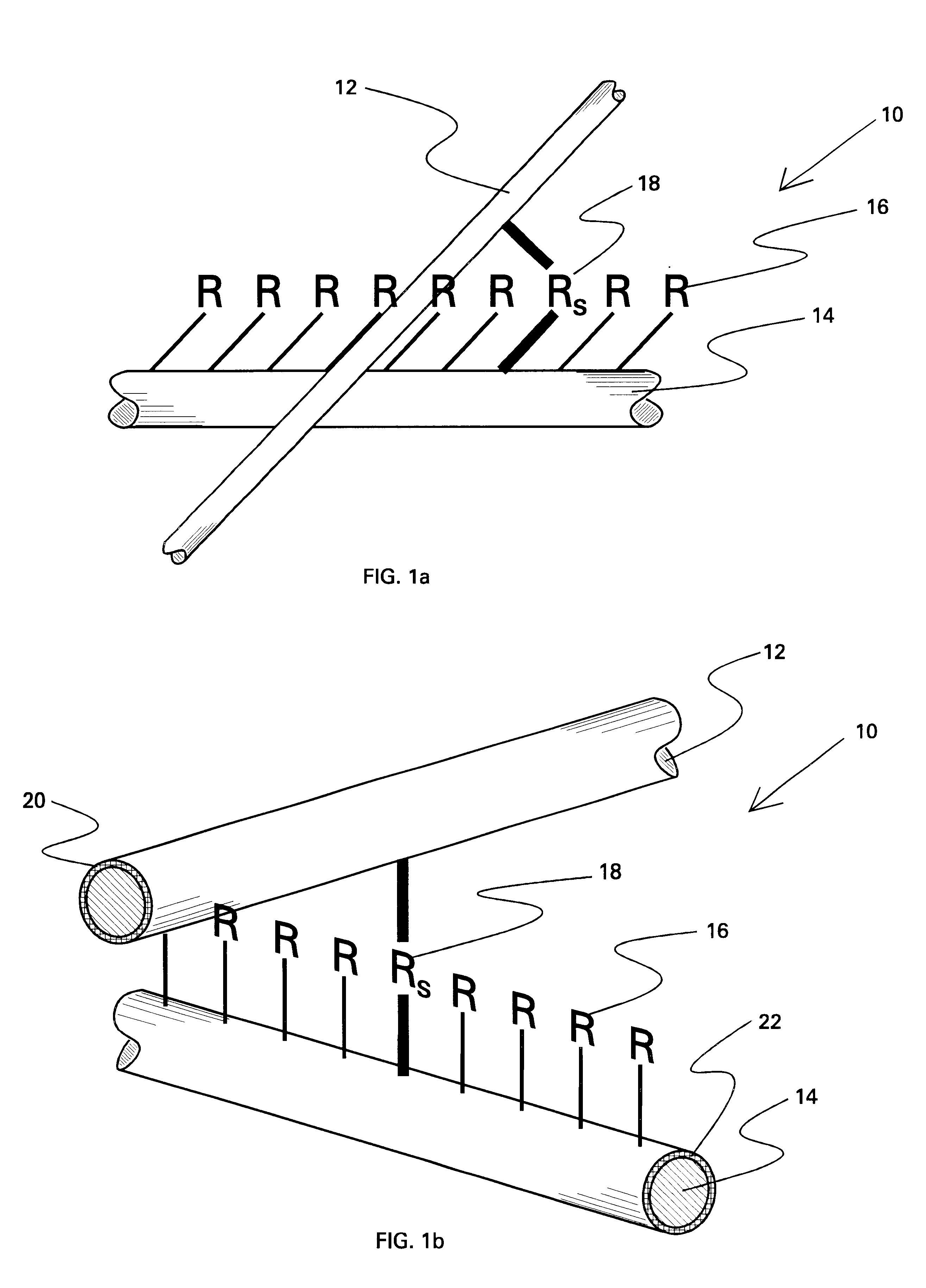
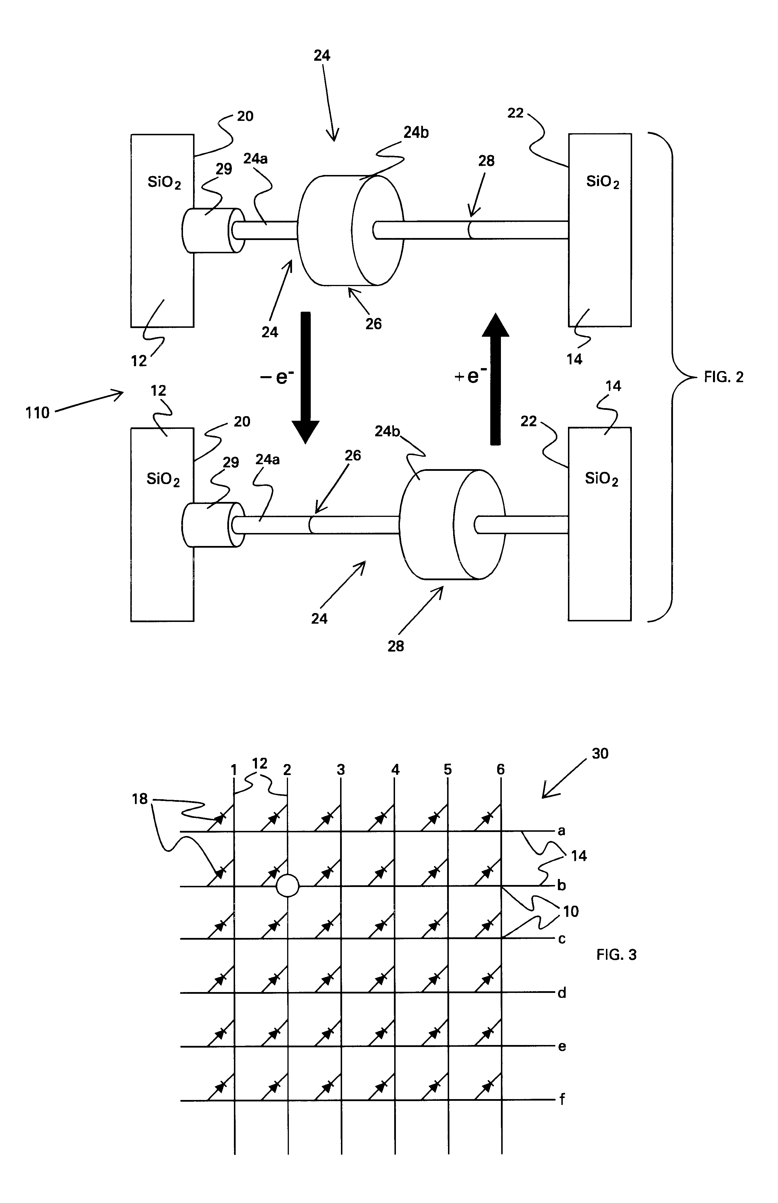
A demultiplexer for a two-dimensional array of a plurality of nanometer-scale switches (molecular wire crossbar network) is disclosed. Each switch comprises a pair of crossed wires which form a junction where one wire crosses another and at least one connector species connecting said pair of crossed wires in said junction. The connector species comprises a bi-stable molecule. The demultiplexer comprises a plurality of address lines accessed by a first set of wires in the two-dimensional array by randomly forming contacts between each wire in the first set of wires to at least one of the address lines. The first set of wires crosses a second set of wires to form the junctions. The demultiplexer solves both the problems of data input and output to a molecular electronic system and also bridges the size gap between CMOS and molecules with an architecture that can scale up to extraordinarily large numbers of molecular devices. Further, the demultiplexer is very defect tolerant, and can work despite a large number of defects in the system.

Description

The present application relates generally to making connections to integrated circuits of electronic devices whose functional length scales are measured in nanometers, and, more particularly, to demultiplexers based on nanometer-scale wires crossed by larger wires and joined by bi-stable molecular scale switches at the intersecting junctions.The silicon (Si) integrated circuit (IC) has dominated electronics and has helped it grow to become one of the world's largest and most critical industries over the past thirty-five years. However, because of a combination of physical and economic reasons, the miniaturization that has accompanied the growth of Si ICs is reaching its limit. The present scale of devices is on the order of tenths of micrometers. New solutions are being proposed to take electronics to ever smaller levels; such current solutions are directed to constructing nanometer scale devices.Prior proposed solutions to the problem of constructing nanometer scale devices have in...

Claims


Application Information

Patent Timeline
Patent Type & Authority Patents(United States)
IPC IPC(8): G11C8/00G11C8/10G11C13/02
CPCB82Y10/00G11C8/00G11C8/10G11C13/02G11C13/0009Y10S977/943G11C2213/14G11C2213/81
Inventor KUEKES, PHILIP J.WILLIAMS, R. STANLEY
Owner HEWLETT-PACKARD ENTERPRISE DEV LP
Learn More