
Semiconductor device and method of manufacturing the same

a semiconductor and semiconductor technology, applied in semiconductor devices, solid-state devices, basic electric elements, etc., can solve the problems of solar battery destruction, glass plate is difficult to apply depending on its usage, and solar battery which becomes unusable must be artificially decomposed when being disposed

Inactive Publication Date: 2001-04-24
SONY CORP
View PDF2 Cites 7 Cited by
  • Summary
  • Abstract
  • Description
  • Claims
  • Application Information

AI Technical Summary

Problems solved by technology

As a result, warp is generated because of the difference in thermal expansion of the solar battery and the plastic plate, resulting in the destruction of the solar battery.
Also, a glass plate is difficult to be applied depending on its usage since it is hard to be folded or to be cut.
Furthermore, as the plastic plate and the glass plate are not spontaneously decomposed, the solar battery which becomes unusable must be artificially decomposed when being disposed.
Therefore, there is a problem of waste disposal such as running cost of decomposing, if solar batteries becomes widespread use in full-scale, and if there are a large amount of the solar batteries which are unusable.

Method used


Image

  • Semiconductor device and method of manufacturing the same
  • Semiconductor device and method of manufacturing the same
  • Semiconductor device and method of manufacturing the same

Examples


second example

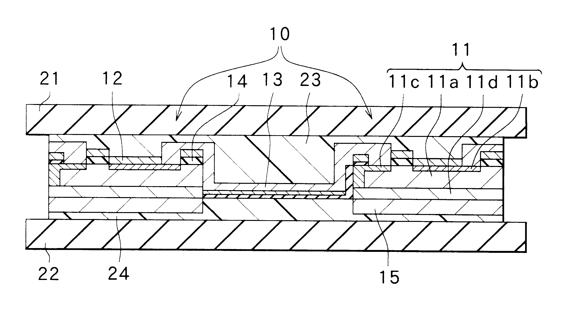
FIG. 5 shows the configuration of a semiconductor device according to a second example of the invention. The semiconductor device has the identical configuration, operation and effects to those of the first example except that it comprises a reflection film 45. Also, it can be formed like the first embodiment. Hence, like elements are given like numerals and the detailed description of them will be omitted.

The reflection film 45 is made of titanium oxide and is formed on the second substrate 22 on the solar batteries 10 side. The reflection film 45 is for increasing the amount of light irradiated into each solar battery 10 by reflecting the light passed through each solar battery 10. At this time, although the reflection film 45 is formed on the second substrate 22 on the solar batteries 10 side, it may be formed on the second substrate 22 on the opposite side of the solar batteries 10. Also, although the reflection film 45 is formed all over the surface, it may be formed on part of...

third example

FIG. 6 shows the configuration of a semiconductor device according to a third example of the invention. The semiconductor device has the identical configuration, operation and effects to those of the first example except that it comprises waterproof films 56 and 57. Also, it can be formed in the same manner as in the first example. Therefore, like elements are given like numerals and the detailed description of them will be omitted.

The waterproof film 56 is formed, for example, on the first substrate 21 on the opposite side of the solar batteries 10, and the waterproof film 57 is formed, for example, on the second substrate 22 on the opposite side of the solar batteries 10. The waterproof films 56 and 57 have a thickness of 20 .mu.m, for example, and it is preferable that they are formed of resin film, respectively. As resin used for the resin film, for example, the following will be suitable: polyolefin resin; polyester resin; melamine resin; silicon resin; or biodegradable resin s...


PUM


Abstract

A plurality of solar batteries are provided between a first substrate and a second substrate. The first substrate and the second substrate are formed of, for example, a paper or a non-woven cloth, which is a material including a natural fiber, cellulose, as the main component. Papers and silicon have relatively small difference in coefficient of thermal expansion so that warp caused by changes in the temperature is suppressed. Also, papers are light, easy to be processed and spontaneously decomposed so that disposing becomes easy. The first substrate is preferable to be transparent or semitransparent and preferable to be formed of cellophane paper, glassine paper, parchment paper, or Japanese paper. Oil may be included in the material. The second substrate is preferable to be opaque. A waterproof film may be formed on the first substrate and the second substrate.

Description

1. Field of the InventionThe present invention relates to a semiconductor device comprising thin film semiconductor layers such as a solar battery and a method of manufacturing the same. Specifically, it relates to a semiconductor device manufactured through forming thin film semiconductor layers on a provisional substrate and then transcribing it on another substrate, and a method of manufacturing the same.2. Description of the Related ArtIn recent years, solar batteries have come to be in practical use. It is necessary to save resources and to decrease costs to utilize solar batteries in full-scale. Thin film solar batteries are preferred to thick film solar batteries when energy conversion (light-electricity) efficiency and shortening the cycle of energy recycle are taken into consideration.The same applicants as this application have first proposed a method of separating an element formation layer from a substrate (Japanese Patent Application laid-open Hei 8-213645). In the meth...

Claims


Application Information

Patent Timeline
Patent Type & Authority Patents(United States)
IPC IPC(8): H01L23/02H01L23/08H01L23/00H01L31/0216H01L31/04H01L31/0203H01L21/20H01L21/36H01L27/14H01L31/00
CPCH01L31/02164H01L31/048H01L31/068H01L31/0465H01L31/056H01L31/0392H01L31/1896Y02E10/547Y02E10/52
Inventor MATSUSHITA, TAKESHIOHARA, SHUZO
Owner SONY CORP
Learn More