
Component carrier having a wave pattern tension reduction surface

Inactive Publication Date: 2001-01-23
IBM CORP
View PDF13 Cites 2 Cited by
  • Summary
  • Abstract
  • Description
  • Claims
  • Application Information

AI Technical Summary

Problems solved by technology

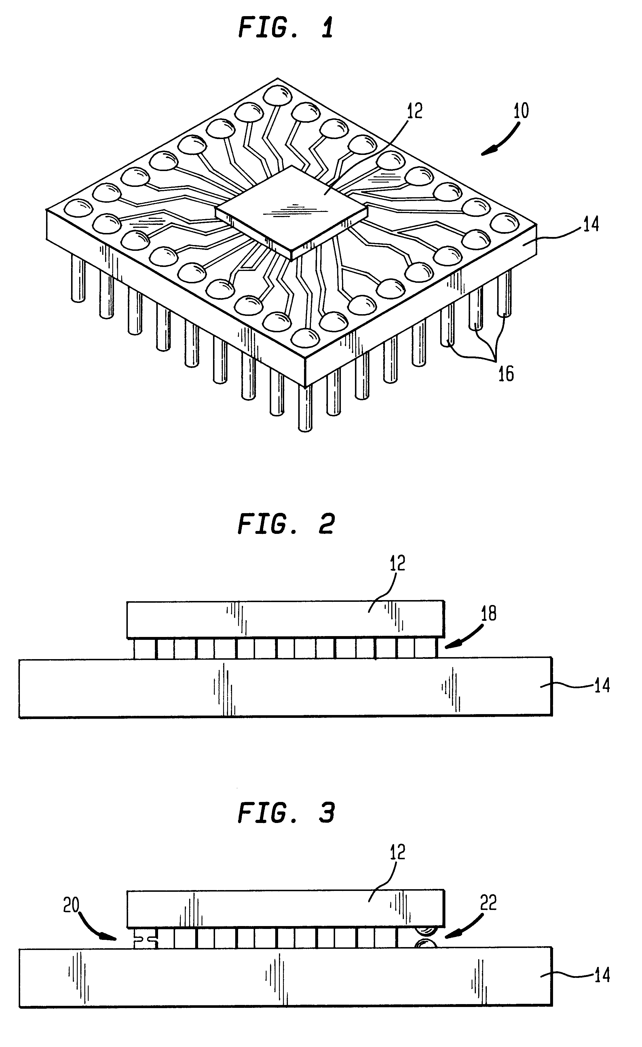
For instance, numeral 20 identifies a nonwet or poor solder joint, which is susceptible to failure subsequent to completion of the device manufacturing process, and further corresponds to a high reliability exposure.
The low volume C4 solder ball pad may have been caused as a result of a good solder ball having been damaged during a previous handling, storage, and/or transportation of the semiconductor die during the manufacturing process.
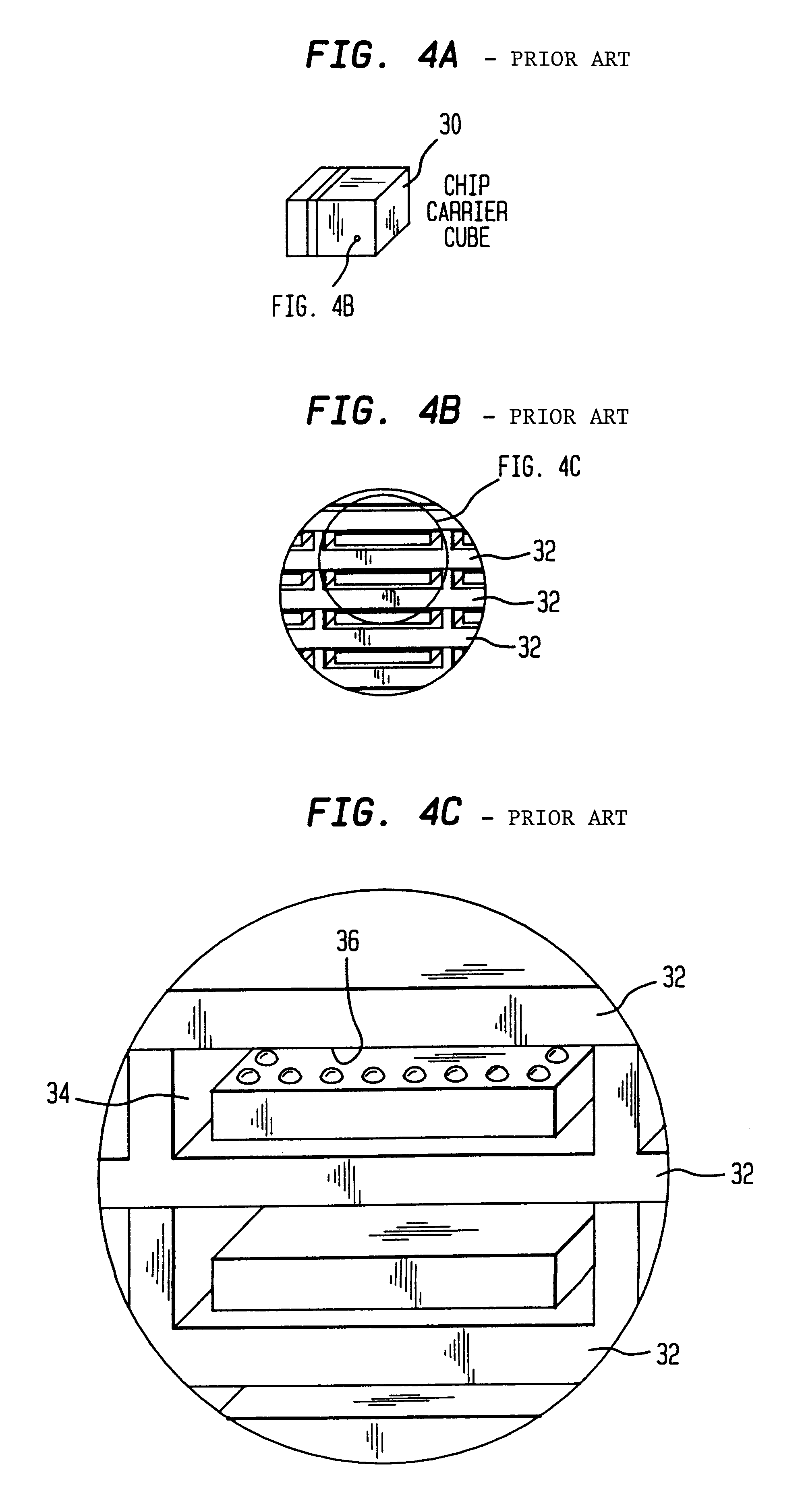
Unfortunately, the textured flat surface becomes smoothed out, by repeated uses and cleaning, over a period of time.
A smoothed out covering surface is undesirable and problematic, since a wire bond die product is subject to sticking thereto due to su

Method used


Image

  • Component carrier having a wave pattern tension reduction surface
  • Component carrier having a wave pattern tension reduction surface
  • Component carrier having a wave pattern tension reduction surface

Examples


Embodiment Construction

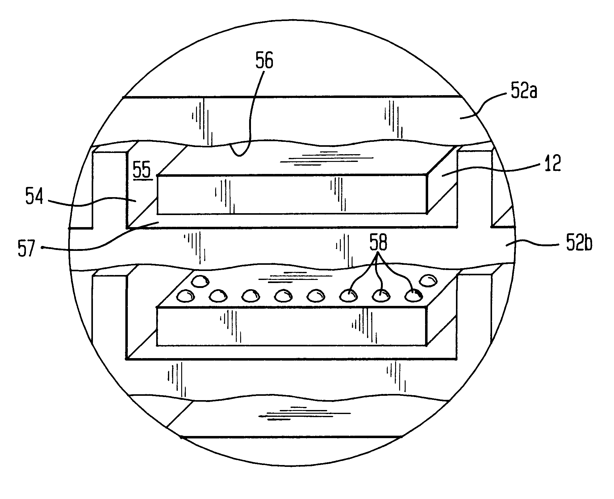
Turning now to FIGS. 6A-6C, a container system 50 for storing and transporting sensitive components, such as semiconductor chips 12, shall be described. Container system 50 includes, in combination, a housing 51 and a plurality of component carriers 52. The component carriers 52 are provided for receiving components 12 to be stored and transported in stacked banks 53. The plurality of component carriers 52 are stacked one on top of the other in a top-to-bottom stacked arrangement within the housing 51. An underside bottom surface 56 of a first component carrier 52a provides a top cover to a second component carrier 5b positioned immediately below the first component carrier 52a.

Each component carrier 52 includes a compartmental core for storing components 12 on a top surface thereof in pockets or segmented row compartments 54. The compartmental core can include, for example, polycarbonate, polypropylene, polystyrene, or any other suitable stable material. Each pocket or segmented ro...


PUM


Abstract

A container system for storing and transporting sensitive components such as semiconductor chips is disclosed. The container system includes in combination, a housing and a plurality of component carriers for receiving components to be stored and transported in stacked banks. The plurality of component carriers are stacked one on top of the other in a top-to-bottom stacked arrangement within the housing. An underside bottom surface of a first component carrier provides a top cover to a second component carrier positioned immediately below the first component carrier, wherein a component carrier includes a compartmental core for storing components on a top surface thereof in segmented row compartments, each segmented row compartment having sidewall surfaces and a bottom surface. The component carrier further includes an underside surface characterized by unidirectional waves having a prescribed wave amplitude and a prescribed wave period, the wave amplitude and wave period selected for simultaneously providing a reduced surface tension to a top surface of a component part and a reduced potential for damage to protruding surface features on a top surface of the component part, respectively, the component part further for being stored in a row compartment of an underlying component carrier in the stacked arrangement.

Description

1. Field of the InventionThis invention relates generally to a container system for storing and transporting of sensitive components such as semiconductor chips, and, more particularly, to a component carrier that provides an improved physically protective environment for the components during storage and shipping.2. Discussion of the Related ArtSemiconductor devices typically comprise one or more semiconductor chips designed for performing a desired function. The manufacture of semiconductor devices begins with the manufacture of the semiconductor chips. The semiconductor chips are first produced in a wafer form and subsequently diced from the wafer into individual chips. The individual chips are then packaged on a suitable substrate. During the device manufacturing process, the semiconductor chips are usually stored temporarily in a chip carrier and transported from one processing station to the next with the chip carrier. At the time the semiconductor chips are stored and transpo...

Claims


Application Information

Patent Timeline
IPC IPC(8): H01L21/67H01L21/673
CPCH01L21/67336H01L21/67356H01L2221/68313B65G49/07
Inventor BLONDIN, JOHN MICHAELJONES, JEFFREY JAYRICH, DAVID J.SMITH, WOODY RAY
Owner IBM CORP
Learn More