Eureka AIR delivers breakthrough ideas for toughest innovation challenges, trusted by R&D personnel around the world.

Process for selective transfer of a microstructure formed on an initial substrate to a final substrate

a microstructure and selective technology, applied in the direction of lamination, decorative surface effects, decorative arts, etc., can solve the problems of increasing difficulty with the size of the component to be transferred, difficulty in transferring the microstructure, and difficulty

Inactive Publication Date: 2000-12-12
COMMISSARIAT A LENERGIE ATOMIQUE ET AUX ENERGIES ALTERNATIVES
View PDF6 Cites 58 Cited by
  • Summary
  • Abstract
  • Description
  • Claims
  • Application Information

AI Technical Summary

Benefits of technology

Another purpose is also to propose a fast and inexpensive transfer process that can be used industrially for series production.
In particular, this type of measure makes automatic assembly of substrates possible using an appropriate machine.

Problems solved by technology

The main problems encountered when making component transfers are related to separation of the component from the initial substrate, and also separation of the component from the intermediate substrate.
There are several difficulties and limitations with this technique.
The first difficulty is related to bringing the intermediate layer into contact with a chemical etching agent, usually a liquid.
The action of the chemical agent is not very efficient, since the intermediate layer is thin and is located between the base part and the surface layer.
This difficulty increases with the size of the component to be transferred, in other word with the extent of the intermediate sacrificial layer.
Furthermore, the need for selecting etching of the intermediate layer without deteriorating the component to be transferred makes it necessary to use particular materials which are not always compatible with the requirements of series production.

Method used


Image

  • Process for selective transfer of a microstructure formed on an initial substrate to a final substrate
  • Process for selective transfer of a microstructure formed on an initial substrate to a final substrate
  • Process for selective transfer of a microstructure formed on an initial substrate to a final substrate

Examples


Embodiment Construction

The purpose of this invention is to propose a process for transferring a microstructure from an initial substrate to a final substrate without any of the difficulties and limitations mentioned above.

One particular purpose is to propose such a process that does not involve etching of an intermediate sacrificial layer or lift-off operation.

Another purpose of the invention is to propose a process enabling selective transfer of one or several regions of a substrate comprising given microstructures, to particular areas on a final substrate.

Another purpose is also to propose a fast and inexpensive transfer process that can be used industrially for series production.

In order to achieve these purposes, the subject of the invention is more precisely a process for transferring at least one microstructure formed on a substrate called the initial substrate, to another substrate called the final substrate.

The process comprises the following steps in sequence:

a) preparation of the initial substra...


PUM

PropertyMeasurementUnit
Thicknessaaaaaaaaaa
Forceaaaaaaaaaa
Electrical conductoraaaaaaaaaa

Abstract

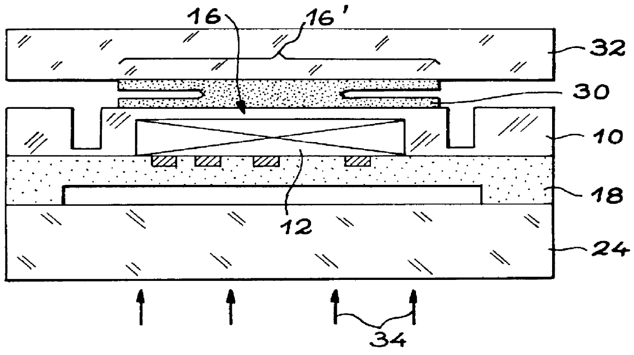
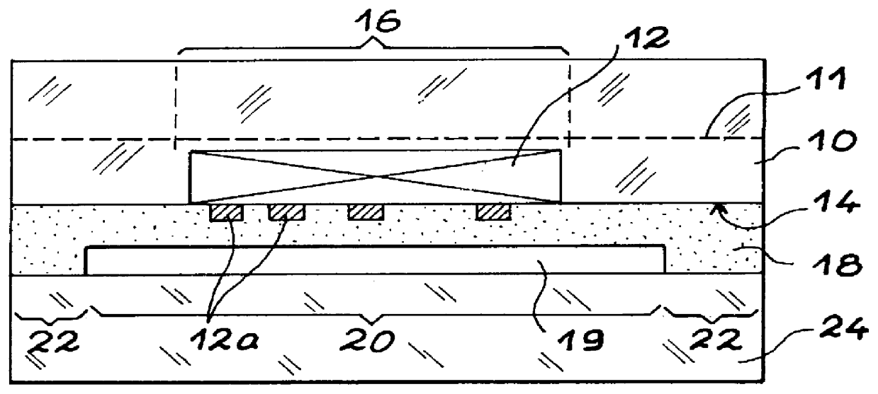
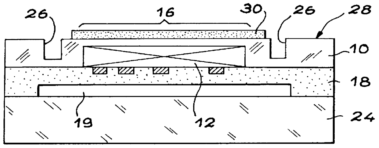
Process for transfer of a microstructure (12) from an initial substrate (10) to a final substrate (32). The process includes the following steps in sequence: bonding between the initial substrate (10) and an intermediate substrate (24), the microstructure facing the intermediate substrate, formation of at least one layer (30) of bond material on at least one selected region (16) of the initial substrate including the microstructure bring the said selected region (16) into contact with the final substrate, treatment of the bond material in an area corresponding to the selected region (16), to increase the bond force, breaking the selected region (16) of the initial substrate, from the intermediate substrate (24).

Description

TECHNICAL DOMAINThis invention relates to a process for selective transfer of a microstructure formed on one substrate called the initial substrate, to another substrate called the final substrate.For the purposes of this invention, a microstructure means any electronic, mechanical or optical component or set of components formed on the initial substrate, by machining, material deposition or material forming techniques specific to microelectronics or micromechanics.In particular, the invention can be used for the transfer of electronic components, that may be passive components or active components such as chips.The transfer of components according to the invention is particularly advantageous in applications in which different components of a device must be made on substrates made of different materials, and in applications for which it is required to manufacture a number of components of a device separately before it is assembled.For example, the invention may be used to transfer ...

Claims


Application Information

Patent Timeline
IPC IPC(8): G02F1/13G02F1/1362H05K3/00H05K3/32H05K3/20
CPCG02F1/13454H05K3/0097H05K3/0058H01L2221/68363
Inventor JOLY, JEAN-PIERRENICOLAS, GERARDBRUEL, MICHEL
Owner COMMISSARIAT A LENERGIE ATOMIQUE ET AUX ENERGIES ALTERNATIVES
Why Eureka
Eureka Blog
Learn More