
Multistage connector for carriers with combined pin-array and pad-array

Inactive Publication Date: 2000-08-22
IBM CORP
View PDF28 Cites 22 Cited by
  • Summary
  • Abstract
  • Description
  • Claims
  • Application Information

AI Technical Summary

Benefits of technology

is to provide such a system which also includes easy reparability of individual contacts for the different contact parts of the socket.
It is yet another object of the present invention to provide an assembly for connecting an IC to a load board which permits simultaneous connection of the test connectors on the IC and the production I / O pins, with zero or low insertion force.

Problems solved by technology

As these devices have become increasingly more dense and complex, the number of I / O connections to a system have also increased, to the point of some multichip modules having hundreds or even thousands of I / Os.
The more complex devices now have large area arrays of contacts, and the forces required to insert and remove a device have become considerable, with increased risk of damage to the device, contact socket, or tester interface board.
This problem led to the development of low-insertion-force (LIF) and zero-insertion-force (ZIF) sockets for devices with pins (Pin Grid Array or PGA), and spring contact compression sockets for devices without pins (Land Grid Array or LGA).
These sockets, while suitable for their intended use, cannot contact a module with both pins and pads incorporated in the module design.
These contacts and sockets, while suitable for their intended use, cannot contact a module with both pins and pads incorporated in the module design.
While this socket contacts PGA and LGA, it cannot contact both simultaneously, and is also not suitable for a large number of contacts.
Commercially available contacting sockets do not provide any suitable solutions to the aforementioned problems.

Method used


Image

  • Multistage connector for carriers with combined pin-array and pad-array
  • Multistage connector for carriers with combined pin-array and pad-array
  • Multistage connector for carriers with combined pin-array and pad-array

Examples


Embodiment Construction

)

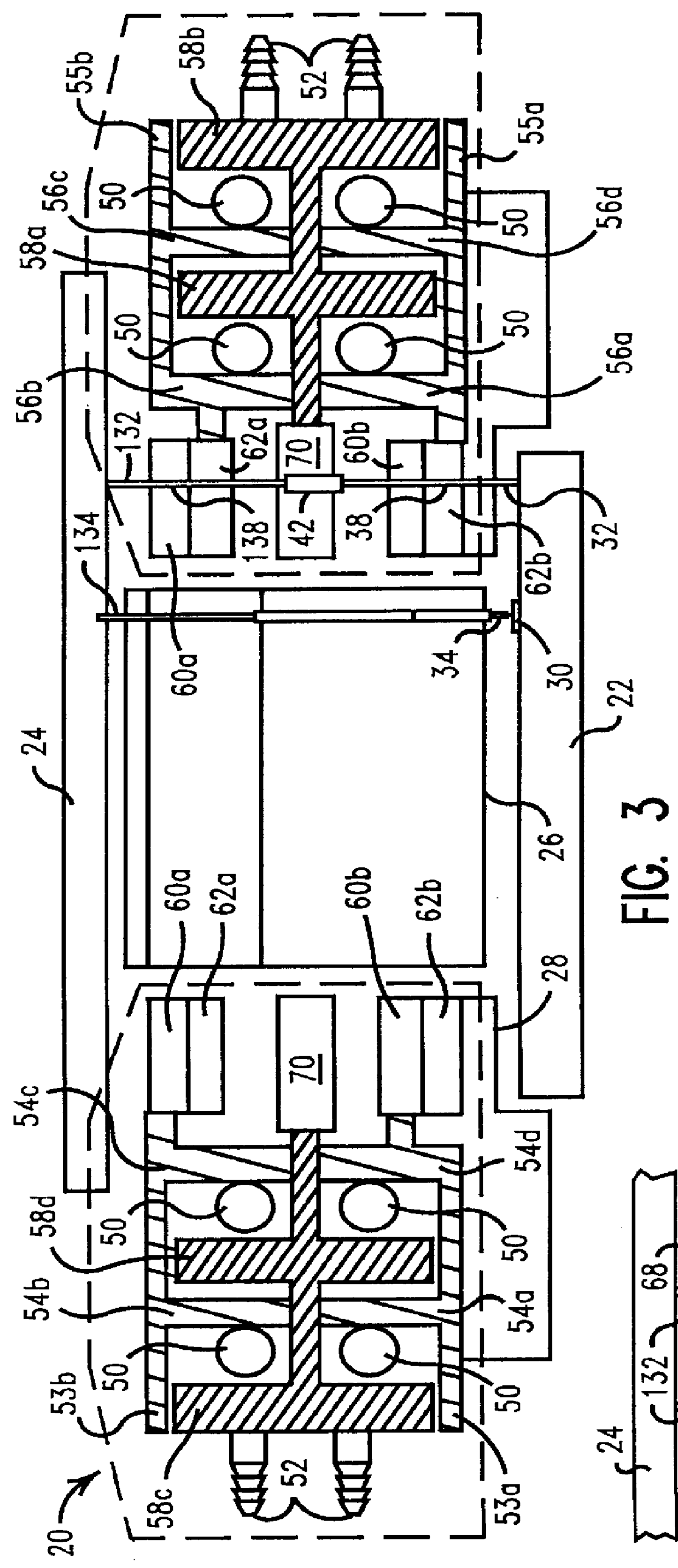
In describing the preferred embodiment of the present invention, reference will be made herein to FIGS. 1-14 of the drawings in which like numerals refer to like features of the invention. Features of the invention are not necessarily shown to scale in the drawings.

The present invention is preferably utilized for connecting a multi-chip integrated circuit module to be tested, also known as a device under testing (DUT), to a circuit board. The preferred connector assembly of the present invention may be utilized with multi-chip module configurations which have the dual requirements of, first, access to internal connections between various circuit dies or chips on the module; and, second, a physical input / output (I / O) pin arrangement on the bottom surface of the module that corresponds to an existing socket design in a computer system. The multistage connector assembly does not require an increase in the number of I / O pins on the module or change in the layout, spacing or signal pin ...


PUM


Abstract

A socket for connecting to an integrated circuit module containing pin grid array contacts and land grid array contacts thereon. The socket has a first portion containing openings therein for the pin grid array contacts and a second portion for contacting the land grid array contacts. The first portion of the socket is disposed around the second portion of the socket, and the second portion is movable with respect to the first portion. The second portion is located in a position wherein the pin grid array contacts on the integrated circuit module are received in the openings in the first portion before the land grid array contacts on the integrated circuit module contact the second portion, the second portion being biased toward the integrated circuit module by a spring. The socket further includes movable connectors in the openings in the first portion of the socket for releasably securing the pin grid array contacts, such that the pin grid array and land grid array contacts on the integrated circuit module are simultaneously in contact with the respective portions of the socket. The connectors comprise leaf connectors movable in a direction lateral to the pin grid array contacts to open while receiving the pin grid array contacts and close to secure the pin grid array contacts in the openings. Inflatable bladders are employed to simultaneously move the leaf connectors between the open and closed positions.

Description

1. Field of the InventionThis invention relates to electronic sockets, and more particularly, to electronic circuit module test sockets for temporarily contacting modules with a combination of pins and pads on the bottom surface that must be contacted simultaneously.2. Description of Related ArtIn the process of manufacturing multi-chip integrated circuit (IC) modules, it is necessary to temporarily make contact to the electrical interface connections (commonly called "pins" or "I / Os") for the purpose of characterization and test. As these devices have become increasingly more dense and complex, the number of I / O connections to a system have also increased, to the point of some multichip modules having hundreds or even thousands of I / Os. Earlier devices with fewer I / Os often had these I / Os arranged around the periphery of the package, and they were easily placed into and removed from a socket with a reasonable amount of force. The more complex devices now have large area arrays of c...

Claims


Application Information

Patent Timeline
IPC IPC(8): H01R13/02H01R12/16H01R13/193H01R12/00H05K7/10H01R12/85
CPCH01R13/193H05K7/1007H01R12/853
Inventor BARRINGER, DENNIS R.CIMINO, KATHRYN M.HAFER, SR., DENNIS J.HORVATH, DREW R.WILSON, STEVEN C.
Owner IBM CORP
Learn More