Split-gate trench mosfet

a technology of split-gate trenches and mosfets, which is applied in the direction of basic electric elements, electrical equipment, semiconductor devices, etc., can solve problems such as production loss

Active Publication Date: 2022-10-06
DIODES INC
View PDF1 Cites 0 Cited by
  • Summary
  • Abstract
  • Description
  • Claims
  • Application Information

AI Technical Summary

Benefits of technology

[0011]An associated technical problem of the split-gate trench MOSFET is that the space between the end of the active trench and the termination trench affects the charge balancing. Experimental results by the Inventors show that when the two ends of an active trench are merged into the termination trench, the reverse bias breakdown performance of the device is less than when both ends are spaced apart from the termination trench, which functions as field plate. In addition, this design increases unbalance between MOSFET cells because it effectively isolates the body region of MOSFET cell from other cell.
[0014]The active trenches are laid out with one end of each trench merged into a termination trench so that the field plate electrode within the termination trench and the filed plate electrode in the active trench are continuous and can stay bias to the same electrical potential. The opposite end of each active trench stands at a distance from an adjacent termination trench so the field plate electrode does not come in contact to the field plate electrode in the adjacent termination trench. The distance may be chosen to maximize the break-down voltage. In some embodiment, the distance is chosen to be the same as the mesa that separates active trenches. The end may be curved, so as the edge of the termination trench adjacent to it. This configuration reduces the electric field density.
[0016]Since one end of each active trench is merged with a termination trench, the field plate electrode in the active trench and the field plate electrode in the termination trench are intimately fixed and the electrical potential at the termination field plate and the active field plate will remain the same. This arrangement frees the MOSFET from having to provide pick-up pads in active trenches. The relocation of the contacts away from the active region guarantees a boost in production yield as the chance of shorting between the gate electrode and the field plate electrode is completely eliminated. In the exemplary MOSFET depicted in the drawing figure, metal leads that carries field plate bias comes to contact directly to the field plate electrode in the termination trenches and through which the field plate electrodes in the active cells are also properly biased.
[0017]Therefore the MOSFET that embody the invention no longer have the yield and reliability issues associated with field plate biasing. And the reverse breakdown issue is improved with engineering the spacing between the second end of the active trench with respect to the adjacent termination trench and by the curvatures at the trench ends and the adjacent area of the termination trenches. Devices of split-gate trench MOSFETs implementing aspects of this invention thus enjoy high manufacture yield and superior device performance.

Problems solved by technology

Due to the close proximity of this gate poly residual and the field plate poly pick-up pad, process tolerance can be severely diminished, which leads directly to loss in production.

Method used


Image

  • Split-gate trench mosfet
  • Split-gate trench mosfet
  • Split-gate trench mosfet

Examples


Embodiment Construction

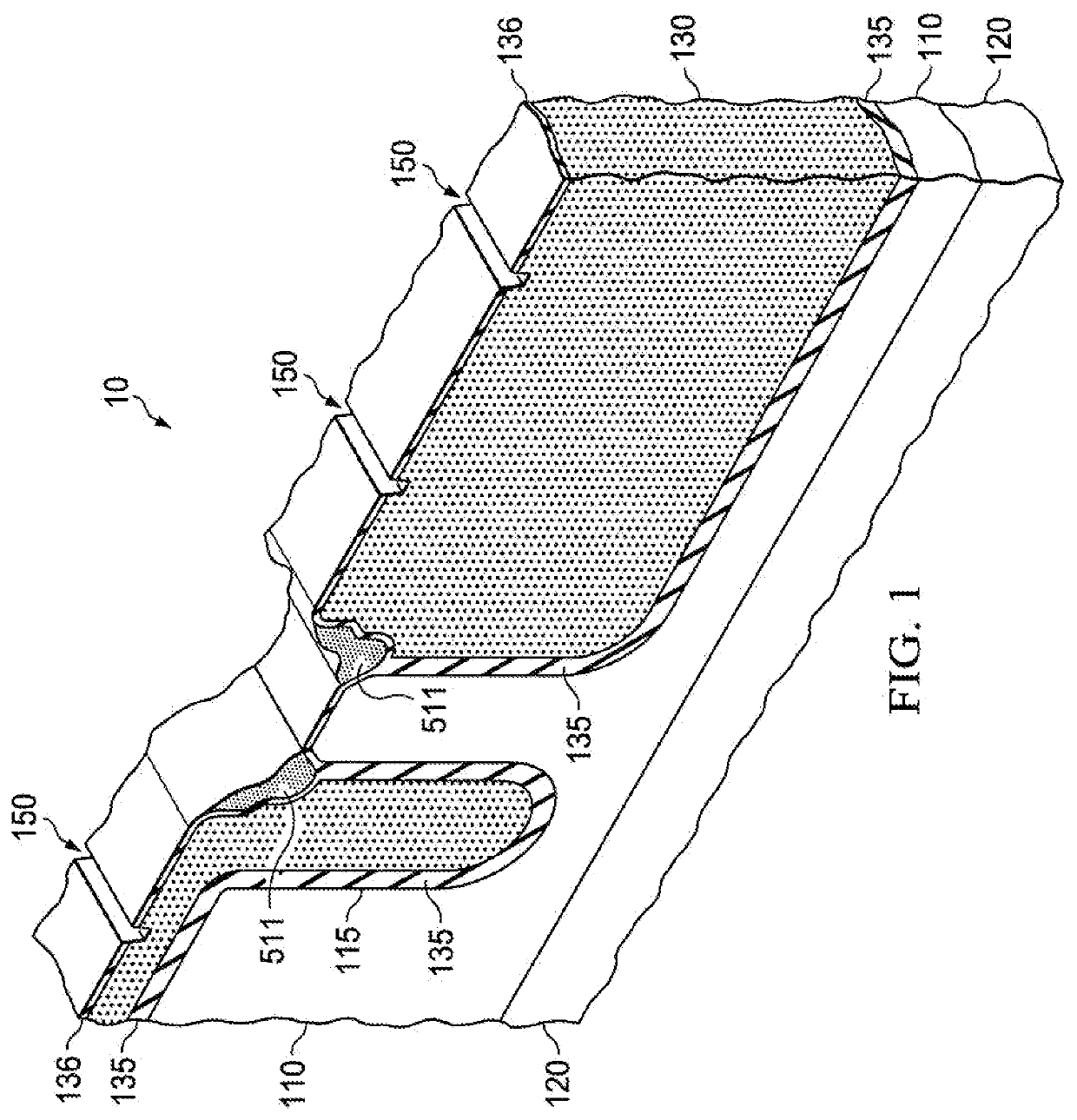
[0069]In drawing FIGS. 1 through 8, various portions of an exemplary silicon based split gate trench MOSFET (metal oxide silicon field effect transistor) and several masks used in making the MOSFET are depicted in the drawings for the purpose of teaching a person skilled in the art to make and use the invention. The drawings are not exhaustive and the elements not to scale but are only for demonstrative purposes.

[0070]FIG. 1 depicts a slice 10 of the MOSFET chip in a perspective sectional view. The slice is within the termination region. At the bottom of drawing is the substrate 120, a silicon layer. It is usually heavily doped with a group V element such as arsenic and phosphorus for a n-type MOSFET; for a p-type MOSFET, the dopant would be of group III such as boron. Over the substrate is an epitaxial (epi) silicon layer of silicon 110. The epi layer is much more lightly doped than the substrate. The thickness of the epi layer is often dictated by the device breakdown voltage. Two...


PUM

PropertyMeasurementUnit
conductiveaaaaaaaaaa
lengthaaaaaaaaaa
areaaaaaaaaaaa

Abstract

A split-gate trench device chip has an active region in which a plurality of active trenches are disposed. The active region is enclosed by termination trenches disposed in a termination region, which extends to the edges of the chip. A gate metal lead is disposed on the device surface. The gate metal lead makes contact to gate electrodes in the active trenches through contact holes disposed in the active region. A source or a drain metal lead is also disposed on the surface. The source or the drain metal lead makes contact to the field plate electrodes through contact holes disposed outside the active region. Each active trench in the active region has a first end merge into a first termination trench and a second end separated from an adjacent second termination trench.

Description

BACKGROUND[0001]There are active cell trenches and termination trenches in a split-gate (or shielded gate) trench MOSFET device chip. Active trenches are aggregated in parallel in the active area at the center of the chip and the termination trenches are at the periphery of the chip surrounding the active cell trenches. The active trenches are laid out as long stripes with lengths coextensive with the length of the active region, and are spaced apart by mesas. Two electrodes are in each active trench—a gate electrode in the upper portion of the trench and a field plate electrode in the lower section. The gate electrode is separated from the sidewalls of the trench by a gate dielectric film, the field plate electrode is separated from the trench sidewall by a field plate dielectric film that is thicker than the gate dielectric film. Both electrodes are conductive and are formed by material such as heavily doped polysilicon. The dielectric films are usually of silicon oxides. Bias vol...

Claims


Application Information

Patent Timeline
Patent Type & Authority Applications(United States)
IPC IPC(8): H01L29/78H01L29/40H01L29/423
CPCH01L29/7813H01L29/407H01L29/4236H01L29/78H01L29/0615H01L29/0684H01L29/42356H01L29/66477H01L29/41766H01L29/0696H01L29/7811H01L29/66734H01L29/42376H01L29/402H01L29/404
Inventor CHUANG, CHIAO-SHUNPAI, TSUNG-WEIKU, YUN-PU
Owner DIODES INC
Why Eureka
Try Eureka