Optically transparent conductor assembly with electrical tracks and touch sensor comprising the same

a conductor and optically transparent technology, applied in the direction of electric digital data processing, instruments, computing, etc., can solve the problems of increasing conductivity, increasing process steps, and strong compromises on transparency

Pending Publication Date: 2022-06-30
SCRONA AG
View PDF17 Cites 0 Cited by
  • Summary
  • Abstract
  • Description
  • Claims
  • Application Information

AI Technical Summary

Benefits of technology

The patent describes a way to make optical assemblies more uniform and easy to manufacture. This is achieved by aligning the tracks on the assembly so that they are parallel to each other, which improves optical homogeneity. The distance between neighboring tracks is either constant or fluctuates over the assembly to reduce the risk of Moiré effects. The track spacing should be distributed so that material coverage over a certain distance doesn't fluctuate by more than 10%. The assemblies can also be covered with optically absorbing cover layers to make them less visible.

Problems solved by technology

Therefore, increasing conductivity comes with strong compromises on transparency.
This involves additional process steps and potentially a reduction of the conductivity if the blackening affects the electrical properties of the metal.

Method used


Image

  • Optically transparent conductor assembly with electrical tracks and touch sensor comprising the same
  • Optically transparent conductor assembly with electrical tracks and touch sensor comprising the same
  • Optically transparent conductor assembly with electrical tracks and touch sensor comprising the same

Examples


Embodiment Construction

Definitions

[0074]A “transparent substrate” or “transparent conductor assembly” is advantageously a substrate or assembly having, for at least a subrange in the visible wavelength range of 400-750 nm, a transmission of at least 50%, in particular of at least 60% or at least 80%. Advantageously, said transmission is spatially uniform across the substrate or assembly and / or uniform over the indicated wavelength range (i.e. the material is colorless).

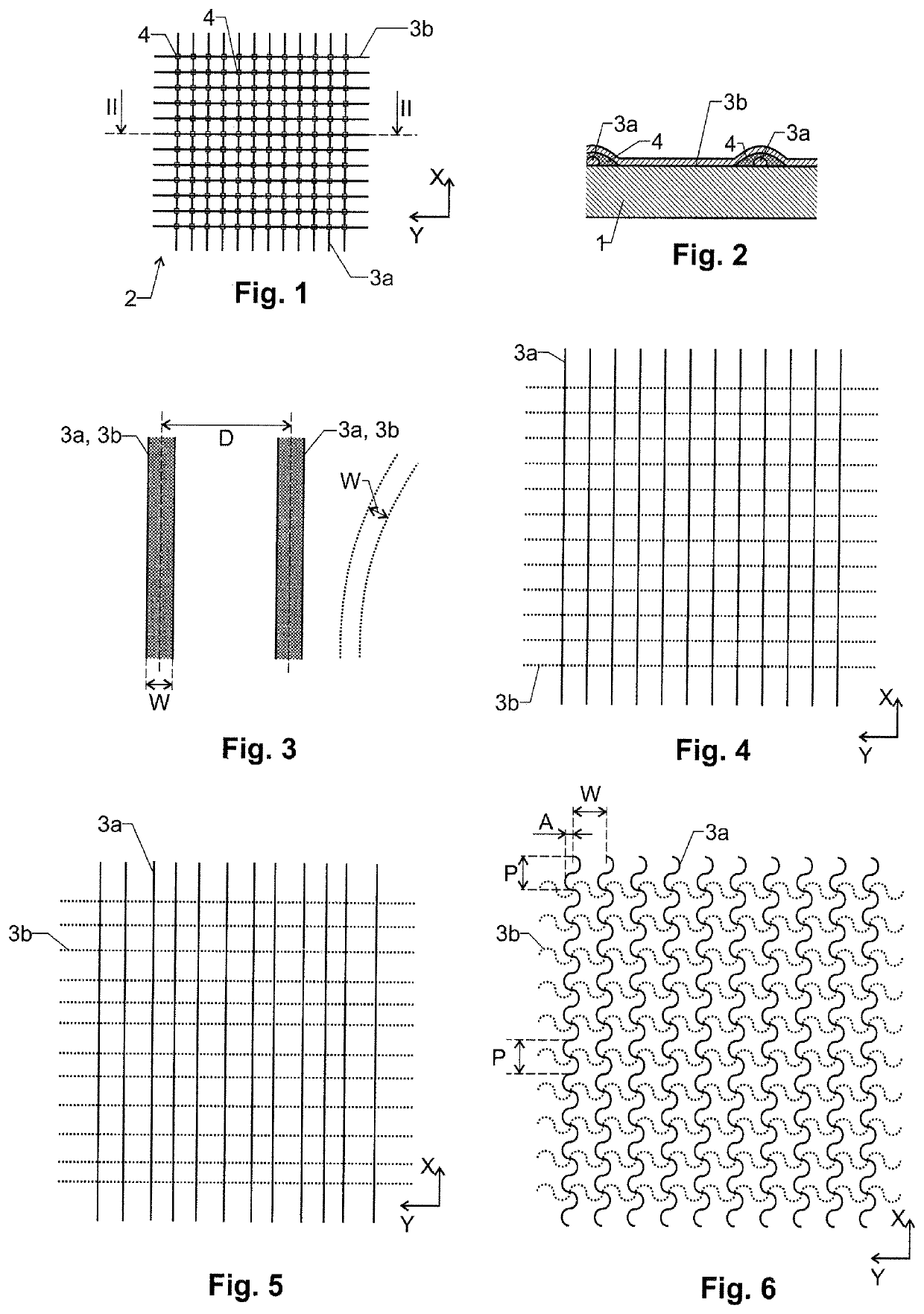
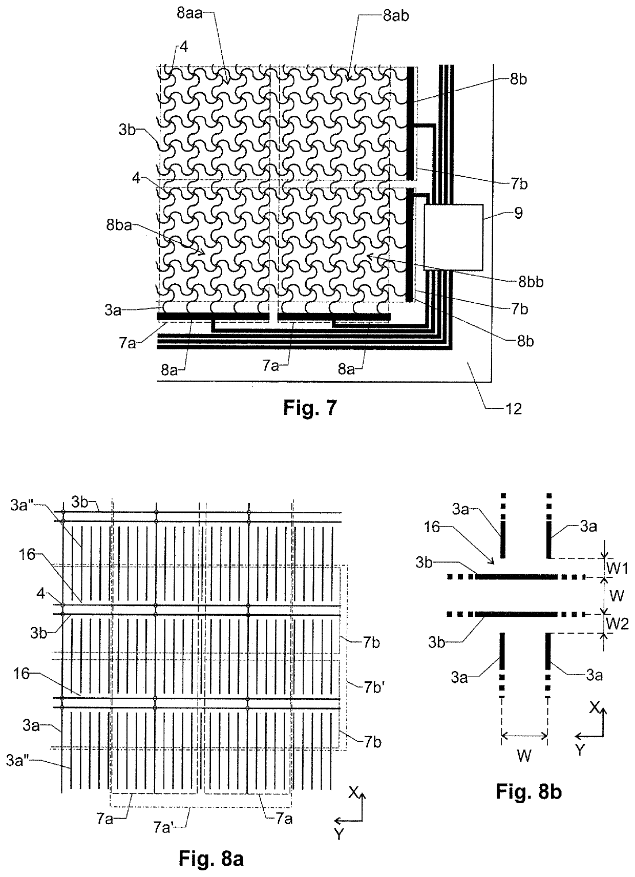
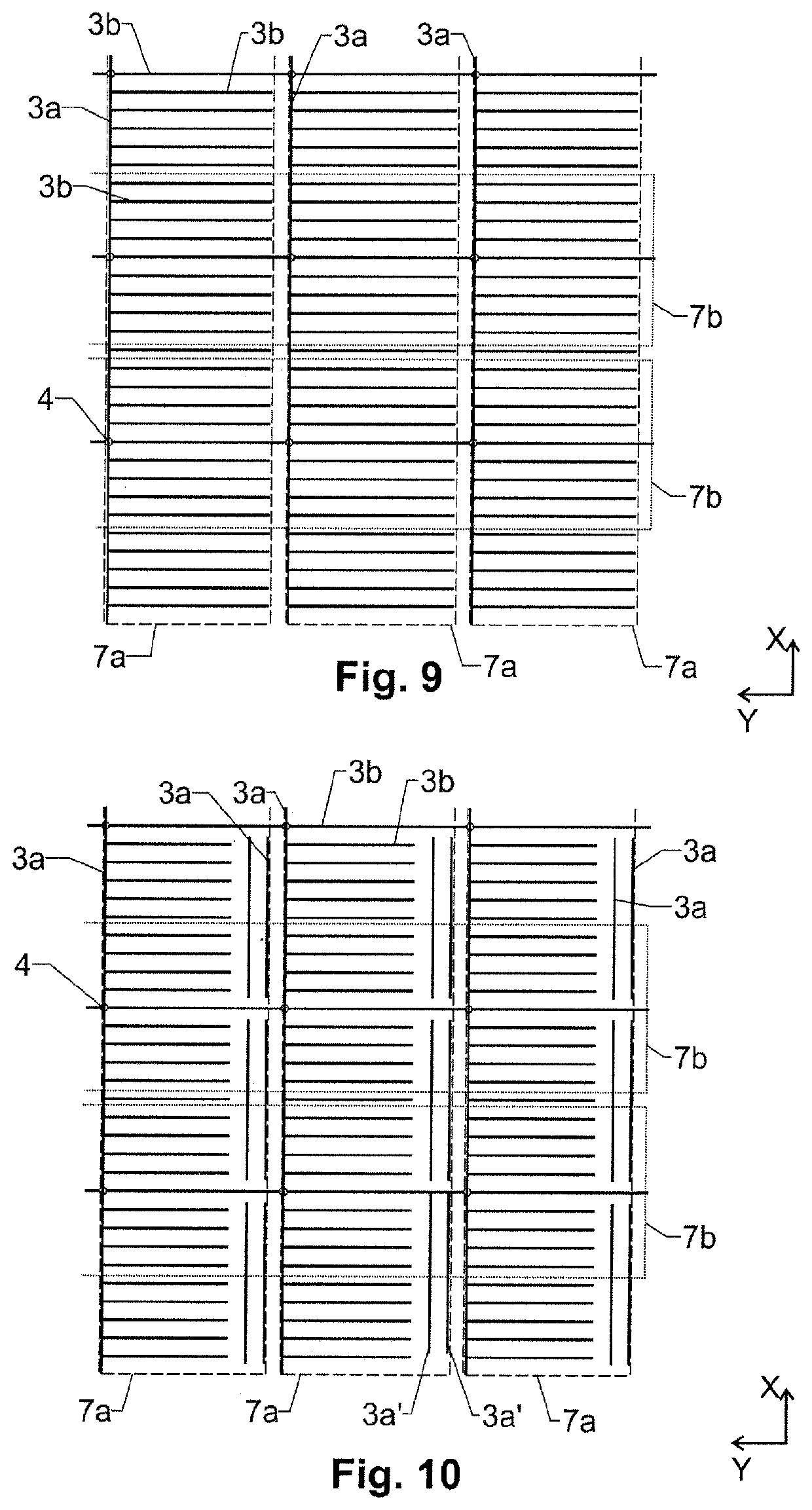
[0075]A “track” is a line of a conducting material having a length much larger than its width.

[0076]A “conducting” material in the present context is advantageously a material having a conductivity of at least 105 S / m at room temperature, in particular at least 106 S / m.

[0077]Conductor Assembly:

[0078]FIGS. 1 and 2 shows a conductor assembly 2 with a single-layer substrate 1.

[0079]Substrate 1 is a transparent body extending along a plane defined by two orthogonal directions X and Y. It advantageously has two parallel outer surfaces parallel t...


PUM

PropertyMeasurementUnit
widthaaaaaaaaaa
distanceaaaaaaaaaa
distanceaaaaaaaaaa

Abstract

A touch sensor has a first and a second set of tracks arranged on a substrate. The tracks have a small width of less than 10 micrometers that renders them invisible to the naked eye. At the same time, neighboring parallel tracks are located at less than 200 micrometers from each other for macroscopic uniformity. The two sets of tracks may include interrupted tracks to reduce mutual capacitance and to increase sensitivity. The tracks can be meandering for optical anisotropy. The touch sensor can be manufactured using electrohydrodynamic ejection printing.

Description

TECHNICAL FIELD[0001]The invention relates to an optically transparent conductor assembly with electrical tracks. It also relates to a spatially resolving capacitive touch sensor comprising said conductor assembly and a touchscreen comprising such a touch sensor, as well as to a method for manufacturing said conductor assembly and touch sensor.BACKGROUND ART[0002]Assemblies of this type are often implemented as so-called metal-mesh transparent conductors (TCs), and they are often used as spatially resolved capacitive touch sensors, e.g. in touchscreens.[0003]They are transparent (in a direction perpendicular to the plane of the substantially 2-dimensional conductor assembly) while still conducting electricity (in a direction along said plane).[0004]One class of such assemblies uses thin film tracks that are conductive and optically transparent at the same time. Such tracks can be made from transparent conductive oxides (TCOs), e.g. indium tin oxide (ITO), and TCs made of this materi...

Claims


Application Information

Patent Timeline
Patent Type & Authority Applications(United States)
IPC IPC(8): G06F3/044
CPCG06F3/0446G06F2203/04103G06F3/0448G06F2203/04112
Inventor GALLIKER, PATRICK
Owner SCRONA AG
Why Eureka
Try Eureka