
Asymmetric Optical Communication Architecture

a communication circuit and optical communication technology, applied in the field of optical communication circuits, can solve the problems of limited bandwidth and is susceptible to noise or interference, and achieve the effect of cost-effective and power-saving

Inactive Publication Date: 2022-06-23
RAFAEL MICROELECTRONICS INC
View PDF8 Cites 0 Cited by
  • Summary
  • Abstract
  • Description
  • Claims
  • Application Information

AI Technical Summary

Benefits of technology

The patent describes a new invention that allows for easier understanding and use of a device or system. The invention includes a detailed description of the device and its features, along with accompanying drawings. This makes it easier for people to understand and use the device, which can improve its overall performance and user-friendliness.

Problems solved by technology

However, conventional cable uses copper wire to transfer video data or control data, which has limited bandwidth and is susceptible to noise or interference.

Method used


Image

  • Asymmetric Optical Communication Architecture
  • Asymmetric Optical Communication Architecture
  • Asymmetric Optical Communication Architecture

Examples


first embodiment

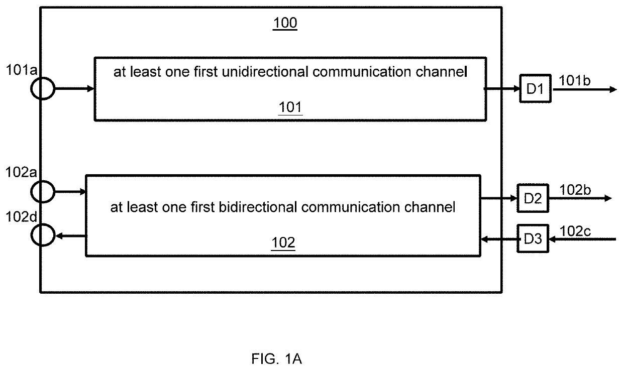
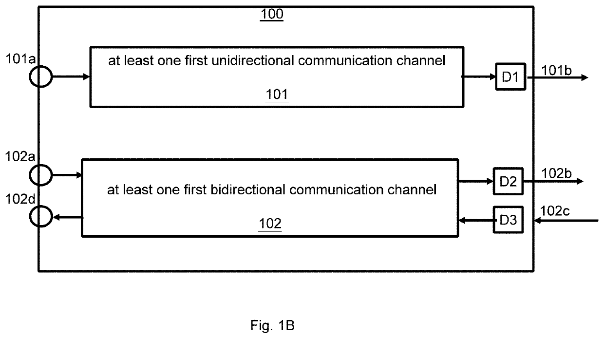
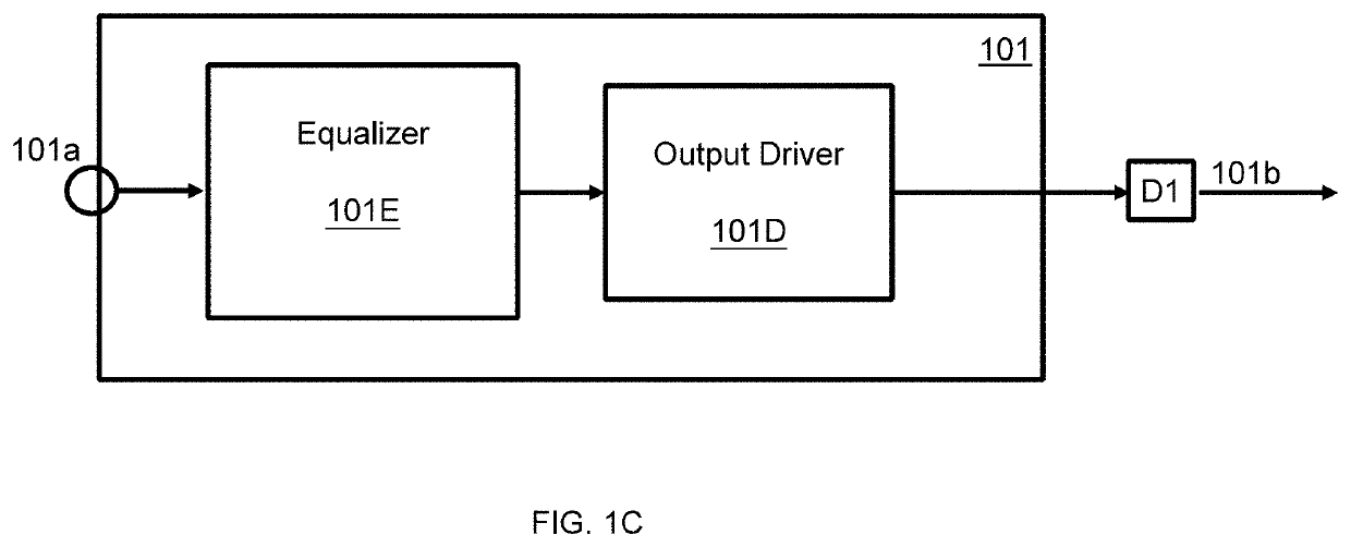
[0062]FIG. 1A illustrates a single-chip integrated circuit 100 with asymmetric optical communication architecture, wherein single-chip integrated circuit 100 comprises: at least one first unidirectional communication channel 101, wherein the first unidirectional communication channel 101 comprises a first sub-circuit for converting a first electrical signal 101a to a first optical signal 101b; and at least one first bidirectional communication channel 102, wherein the first bidirectional communication channel comprises a second sub-circuit for converting a second electrical signal 102a to a second optical signal 102b and a third sub-circuit for converting a third optical signal 102c to a third electrical signal 102d.

[0063]In one embodiment, the first electrical signal 101a is a single-ended signal, wherein a pin of the single-chip integrated circuit 100 is used for inputting the first electrical signal 101a.

[0064]In one embodiment, the first electrical signal 101a is a pair of dif...

second embodiment

[0102]FIG. 3A illustrates a single-chip integrated circuit 300, wherein single-chip integrated circuit 300 comprises: at least one first unidirectional communication channel 301, wherein the first unidirectional communication channel 301 comprises a first sub-circuit for converting a first optical signal 301b to a first electrical signal 301a; and at least one first bidirectional communication channel 302, wherein the first bidirectional communication channel comprises a second sub-circuit for converting a second electrical signal 302a to a second optical signal 302b and a third sub-circuit for converting a third optical signal 302c to a third electrical signal 302d.

[0103]In one embodiment, a pin of the single-chip integrated circuit 300 is used for outputting the first electrical signal 301a, wherein the first electrical signal 301a is a single-ended signal.

[0104]In one embodiment, the first electrical signal 301a is a pair of differential signals, wherein two pins of the single-c...


PUM


Abstract

A single-chip integrated circuit is disclosed, wherein the single-chip integrated circuit comprises at least one unidirectional communication channel for converting a first electrical signal to a first optical signal and at least one bidirectional communication channel for converting a second electrical signal to a second optical signal and converting a third optical signal to a third electrical signal.

Description

BACKGROUND OF THE INVENTION1. Field of the Invention[0001]The invention relates to an optical communication circuit, and in particular, but not exclusively, to an optical communication circuit with asymmetric optical communication architecture.2. Description of the Prior Art[0002]In recent years, optical fiber has been widely used for transmitting video signals or other high data rate signals. However, conventional cable uses copper wire to transfer video data or control data, which has limited bandwidth and is susceptible to noise or interference.[0003]Accordingly, the present invention proposes a better solution to overcome the above-mentioned problems.SUMMARY OF THE INVENTION[0004]One objective of the present invention is to provide a single-chip integrated circuit with asymmetric optical Communication architecture to provide cost effective and power efficient solution for AOC (Active Optical Cable) applications.[0005]The present invention discloses a single-chip integrated circu...

Claims


Application Information

Patent Timeline
Patent Type & Authority Applications(United States)
IPC IPC(8): H04L25/03H04L25/02H04B10/40
CPCH04L25/03885H04L25/03057H04B10/40H04L25/03343H04L25/0272H04N7/22H04N5/765H04N7/015H04B10/2589
Inventor CHEN, CHIA-HSIOUKAN, MENG-PINGHSIEH, CHUN-AN
Owner RAFAEL MICROELECTRONICS INC
Learn More