Display panel, manufacturing method of same, and tiled display panel
a technology of display panel and manufacturing method, applied in the field of display, can solve the problems of reducing display quality, increasing screen size, and increasing manufacturing difficulty and manufacturing cost per unit area, and achieve the effect of eliminating or reducing seams
- Summary
- Abstract
- Description
- Claims
- Application Information
AI Technical Summary
Benefits of technology
Problems solved by technology
Method used
Image
Examples
first embodiment
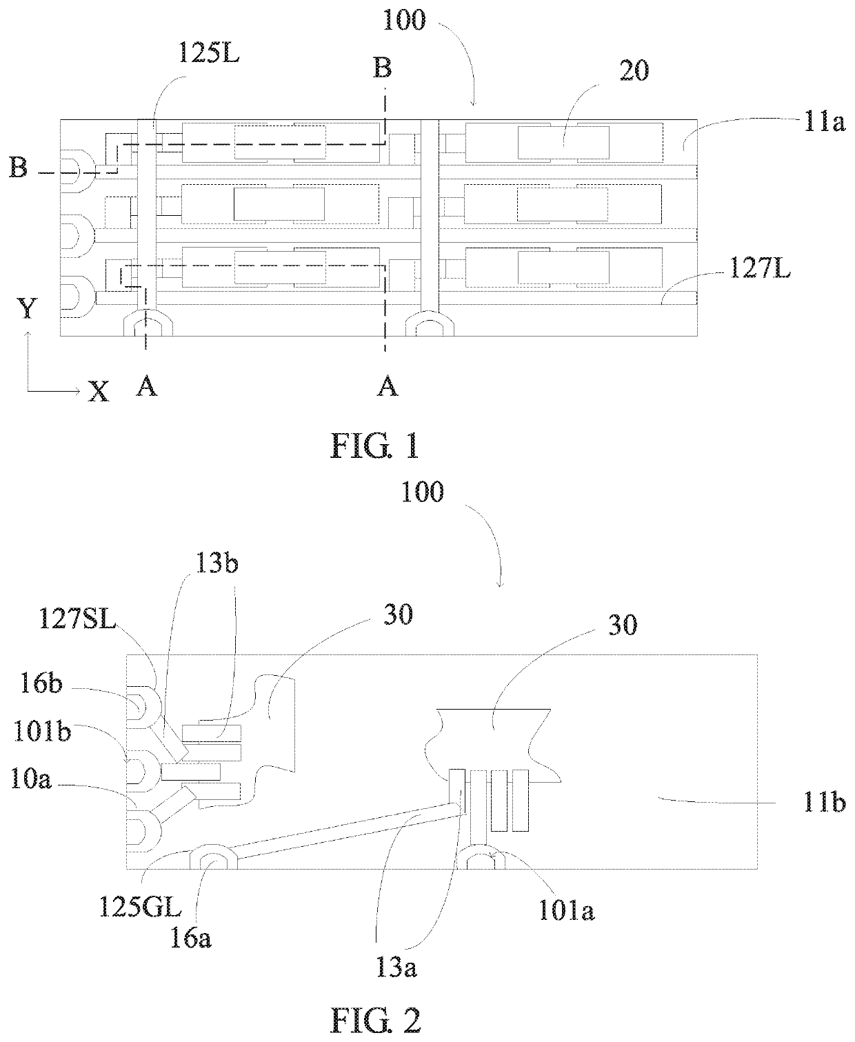
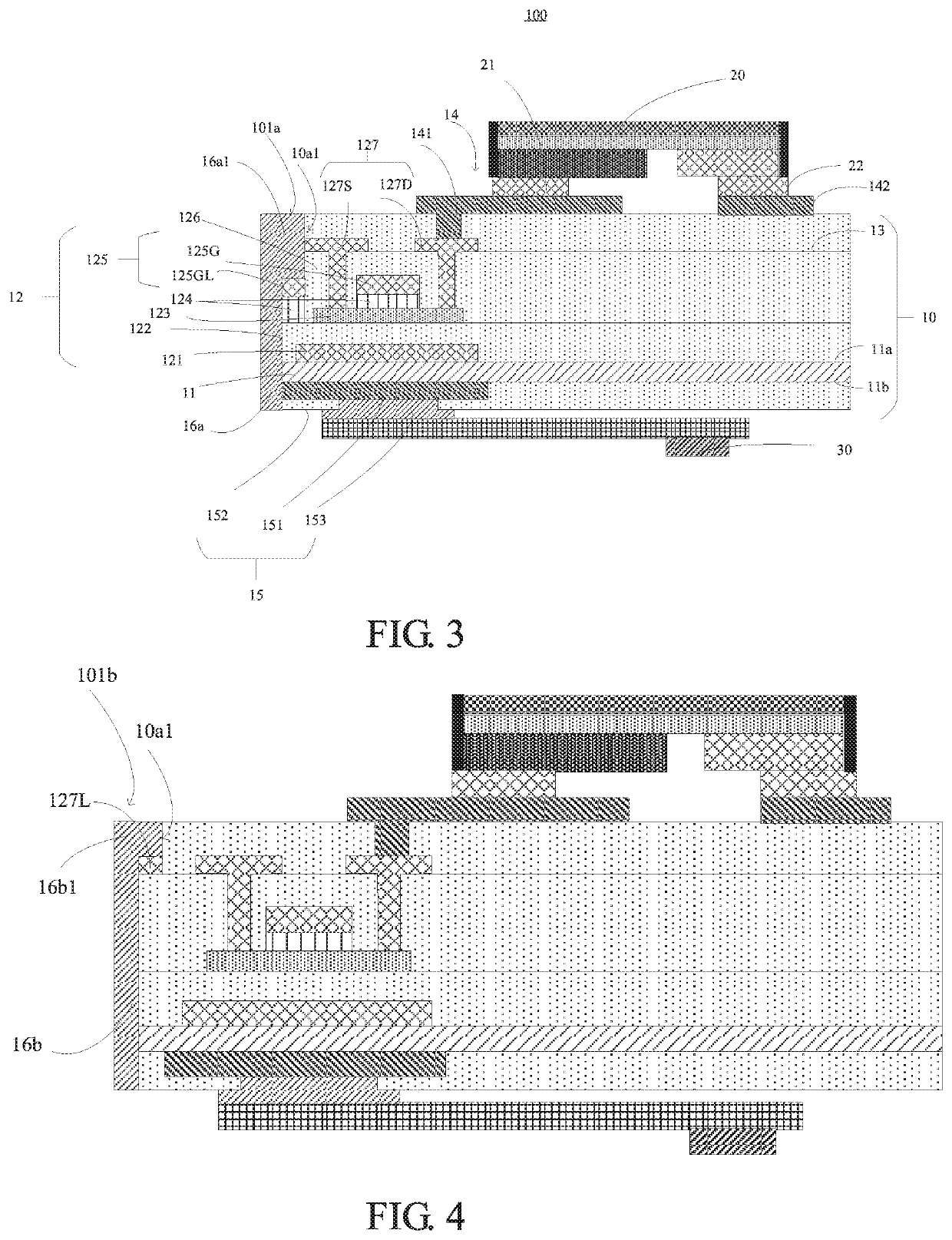
[0098]Thus, the display panel 100 provided by this disclosure is obtained.
[0099]In other embodiments of the present disclosure, the array substrate can also comprise a common electrode line, a power supply and voltage line, and other signal lines used to transmit signals, and the driver chip can also comprise a power supply chip and other driver chips. Similarly, by the same method of providing the openings on the edges of the array substrate and forming the electrical connection parts in the openings to electrically connect the driver chip, the fanout circuit and the signal lines, a display area becomes closer to a bezel area, so as to achieve an effect of bezel-free or narrow-bezel.
third embodiment
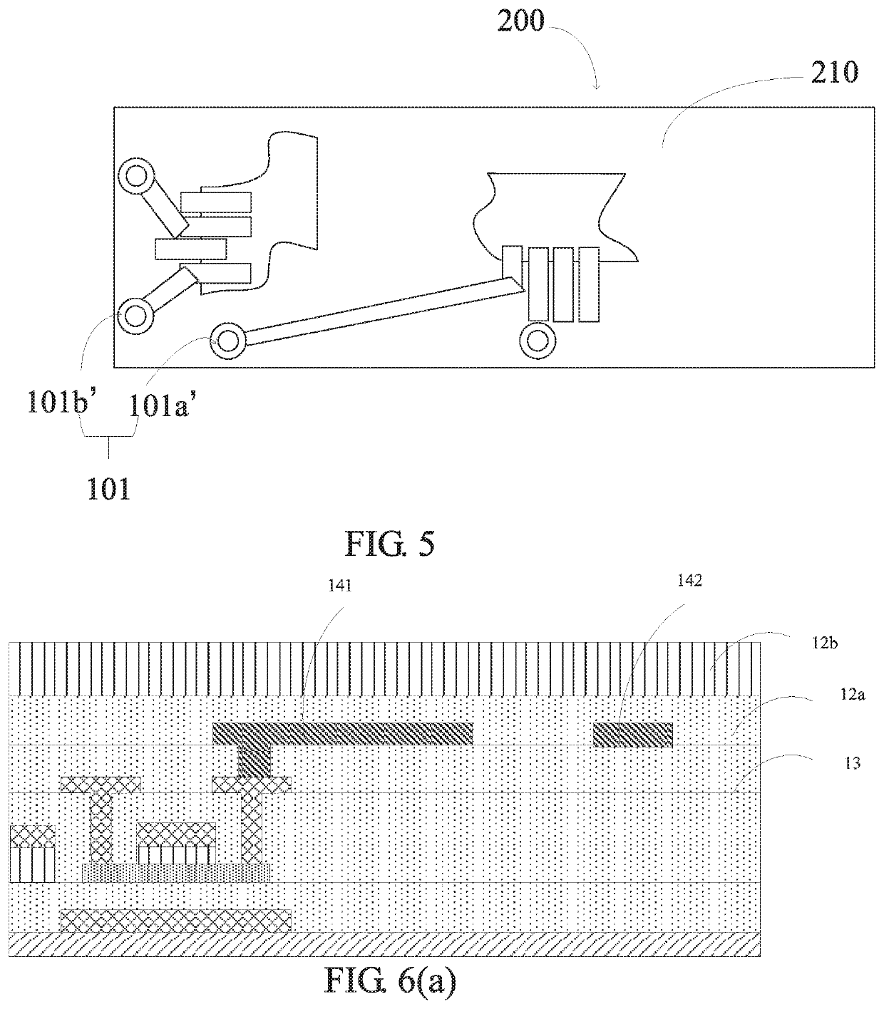
[0100]A tiled display panel 1 according to the present disclosure comprises a plurality of display panel 100 tightly arranged in a matrix. The plurality of display panel 100 is bezel-free or narrow-bezel panel, therefore, there is no apparent seams in the tiled display panel 100.
[0101]The above-mentioned bezel-free display panel or narrow-bezel display panel 100 are applied in a tiled display panel 1 according to the third embodiment of the present disclosure, so that seams can be narrowed to a size of one-pixel unit, so as to make the seams difficult to be recognized by the naked eye by users and achieve an effect of eliminating or reducing seams.
[0102]The above-mentioned embodiments only list micro LED type display panels, but it can be understood that the application can also be used in other active light-emitting type display panels. For example, the application can be used in organic light-emitting diode (OLED) display panels. That is to say, an organic light-emitting component...
PUM
| Property | Measurement | Unit |
|---|---|---|
| transparent | aaaaa | aaaaa |
| size | aaaaa | aaaaa |
| electrical | aaaaa | aaaaa |
Abstract
Description
Claims
Application Information
 - R&D
- Intellectual Property
- Life Sciences
- Materials
- Tech Scout
- Unparalleled Data Quality
- Higher Quality Content
- 60% Fewer Hallucinations
Browse by: Latest US Patents, China's latest patents, Technical Efficacy Thesaurus, Application Domain, Technology Topic, Popular Technical Reports.
© 2025 PatSnap. All rights reserved.Legal|Privacy policy|Modern Slavery Act Transparency Statement|Sitemap|About US| Contact US: help@patsnap.com


