Analog switch

Active Publication Date: 2021-04-22
ABLIC INC
View PDF0 Cites 0 Cited by
  • Summary
  • Abstract
  • Description
  • Claims
  • Application Information

AI Technical Summary

Benefits of technology

The analog switch described in this patent is designed to handle high signal voltages without making the circuit larger or using more power than previous versions. This is a technical improvement that helps in reducing power consumption while maintaining the functionality of the analog switch.

Problems solved by technology

However, a MOS transistor having a high withstand voltage is large in scale and amount of power consumption as compared to a MOS transistor having a relatively low withstand voltage.
This means that the analog switch configured to switch a signal having a high signal voltage is relatively large in circuit scale and amount of power consumption.

Method used


Image

  • Analog switch
  • Analog switch
  • Analog switch

Examples


Embodiment Construction

"d_n">[0038]Now, analog switches according to at least one embodiment of the present invention are described with reference to the drawings.

[0039]Each of the analog switches according to the at least one embodiment is configured to connect or disconnect an electrical path between one terminal selected from at least one signal input terminal containing a first signal input terminal and one terminal selected from at least one signal output terminal containing a first signal output terminal. First, of the analog switches according to the at least one embodiment, description is given of an analog switch including one signal input terminal as the at least one signal input terminal, to which a signal to be switched is supplied, and one signal output terminal as the at least one signal output terminal, from which a signal is output.

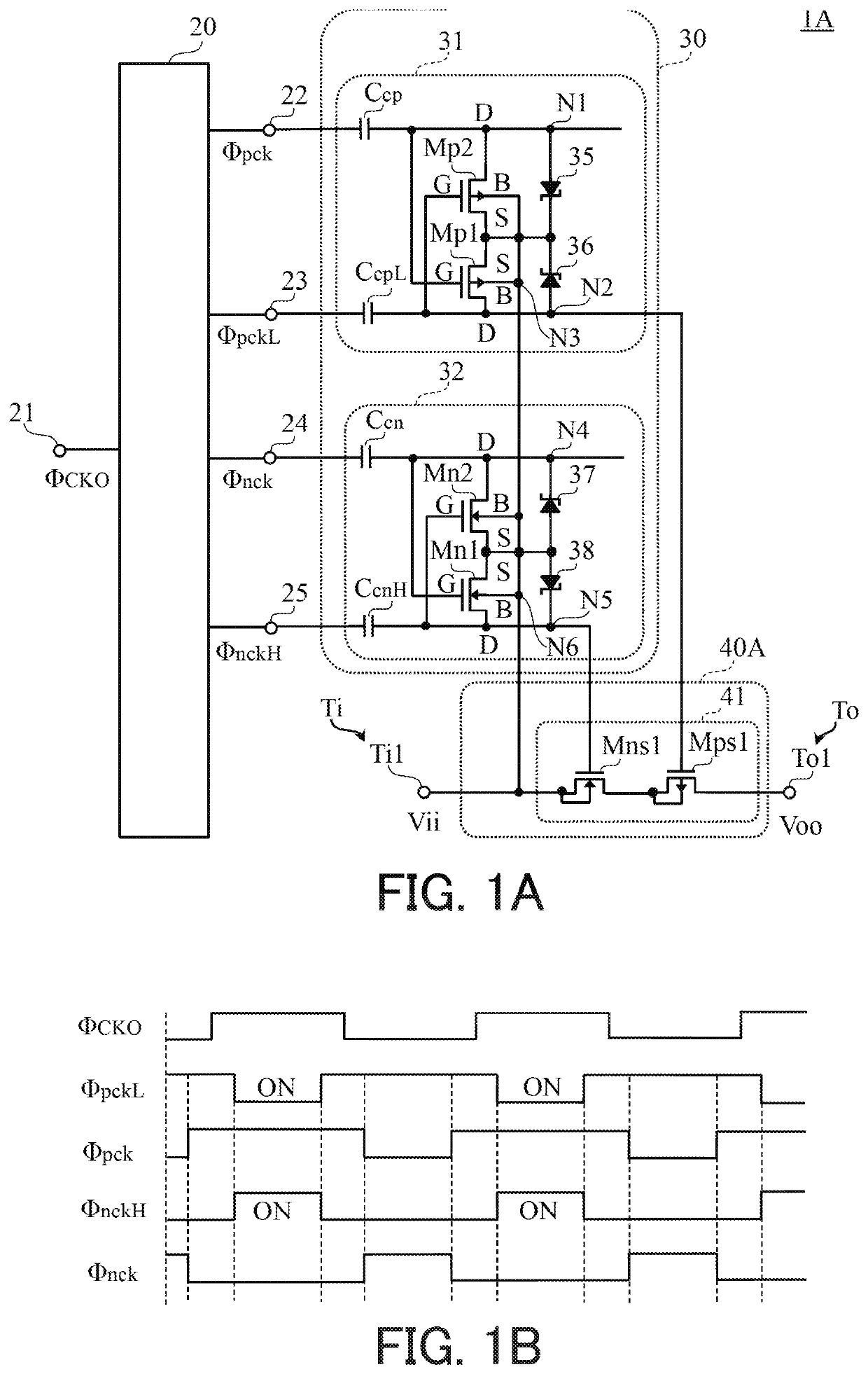
[0040]FIG. 1A is a circuit diagram for illustrating a configuration of an analog switch 1A, and FIG. 1B is a timing chart of clocks ΦCKO, Φpck, ΦpckL, Φnck, and...


PUM


Abstract

The analog switch includes: a clock generation circuit configured to generate a first clock and a second clock; a transfer circuit including an NMOS transistor having a source and a back gate connected to each other, and a PMOS transistor having a source and a back gate connected to each other, one of which has a drain connected to the source of the other, and a source connected to a signal input terminal, and the other of which has a drain connected to a signal output terminal; a first control signal generation circuit configured to generate a control signal for switching the PMOS transistor based on a voltage at the signal input terminal and the first clock; and a second control signal generation circuit configured to generate a control signal for switching the NMOS transistor based on the voltage at the signal input terminal and the second clock.

Description

RELATED APPLICATIONS[0001]This application claims priority to Japanese Patent Application No. 2019-191404, filed on Oct. 18, 2019, the entire content of which is incorporated herein by reference.BACKGROUND OF THE INVENTION1. Field of the Invention[0002]The present invention relates to an analog switch.2. Description of the Related Art[0003]As an example of an analog switch configured to transmit an electric signal, there is known an analog switch using a MOS transistor which is a semiconductor element. The analog switch using the MOS transistor is configured to switch a signal having a signal voltage in a range of from about several V to about 1,000 V depending on its use. In a case where the voltage of the signal to be switched is relatively high such as 100 V, the analog switch is formed of a MOS transistor having a withstand voltage that is equal to or higher than the signal voltage. Analog switches each formed of such a MOS transistor having a relatively high withstand voltage a...

Claims


Application Information

Patent Timeline
IPC IPC(8): G06F1/08H03K17/687
CPCG06F1/08H03K17/6874H03K17/6872H03K17/063H03K2217/0054
Inventor IMAIZUMI, EIKI
Owner ABLIC INC
Why Eureka
Try Eureka