Display device
- Summary
- Abstract
- Description
- Claims
- Application Information
AI Technical Summary
Benefits of technology
Problems solved by technology
Method used
Image

Examples
embodiment 1
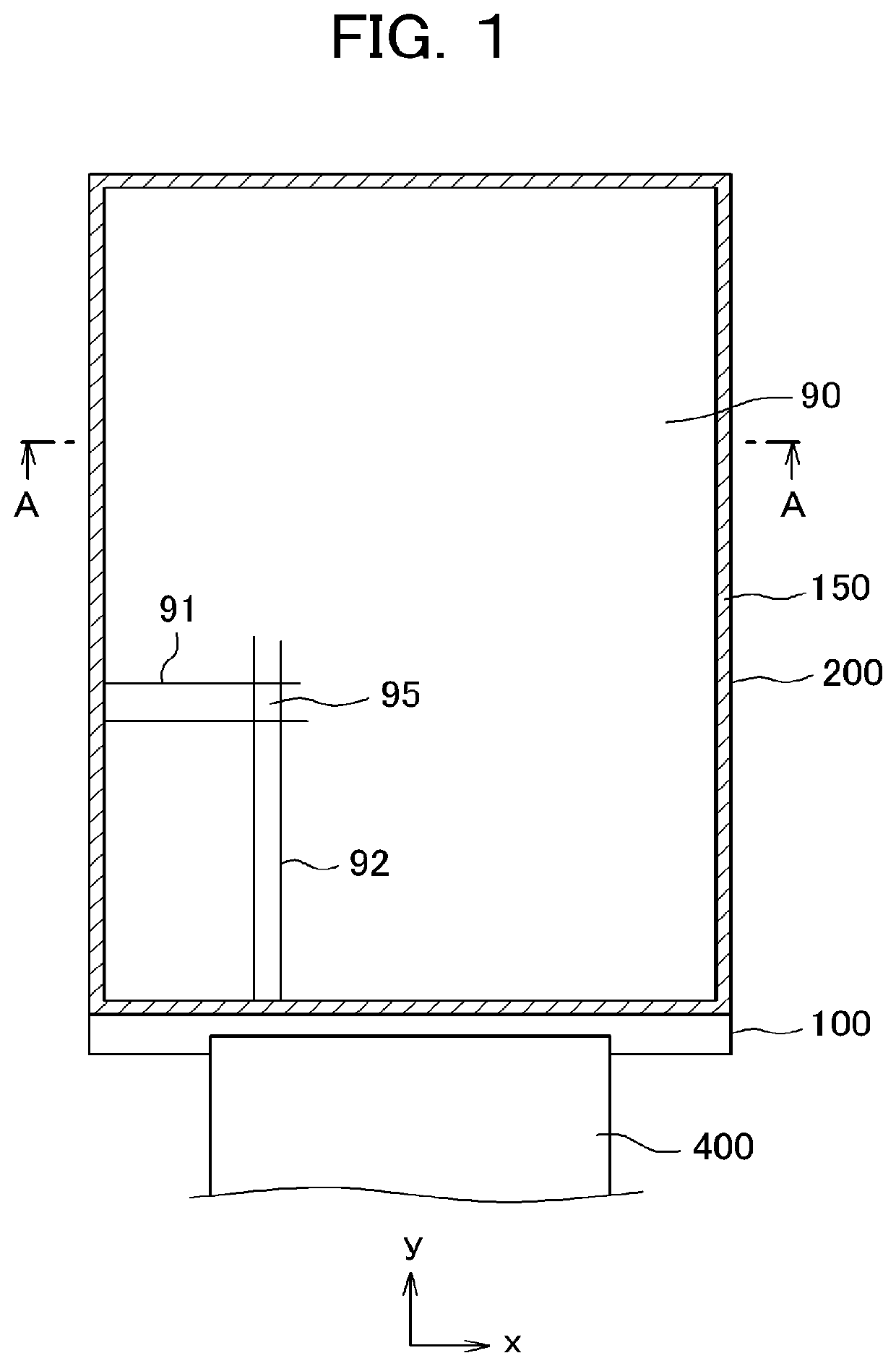
[0056]FIG. 1 is a plan view of the liquid crystal display device, in which the present invention is applied. The present invention can be used in a display device, which is bendable flexibly. Therefore, the TFT substrate 100, on which the scan signal lines, the video signal lines, the pixels, and so forth are formed, is made of the resin substrate. Among resins, polyimide has excellent characteristics for the substrate of the display device because of its heat resistance, mechanical strength, and so forth. Therefore, the polyimide is premised to be used for the TFT substrate 100 herein after; however, the present invention is applicable even when the TFT substrate 100 is made of other resins.
[0057]FIG. 1 is a plan view of the liquid crystal display device. In FIG. 1, the TFT substrate 100 and the counter substrate 200 are mutually adhered by the sealant 150; the liquid crystal is sandwiched between the TFT substrate 100 and the counter substrate 200, and is sealed inside of the seal...
embodiment 2
[0078]FIG. 11 is a cross sectional view of embodiment 2 according to the present invention. FIG. 11 differs from FIG. 8 of embodiment 1 in that the aluminum oxide layer 14 (herein after AlO layer) is formed between the polyimide substrate 100 and the adhesion layer 11, which is formed from nitride. The adhesion layer 11 is formed for adhesion between the a-Si layer 12 and the polyimide substrate 100; however, there is an occasion that the adhesive strength is not enough between the polyimide substrate 100 and the adhesion layer 11. In embodiment 2, the AlO layer 14, which has a high adhesive strength with the polyimide substrate 100, is formed between the adhesion layer 11 and the polyimide substrate 100; thus, adhesive strength between the polyimide substrate 100 and the multilayer film 20 is more stabilized. In other words, two layers of the adhesion layer 11 and the Al layer 14 are used for the adhesion layer in embodiment 2.
[0079]The reaction shown in FIG. 12 explains how the ad...
embodiment 3
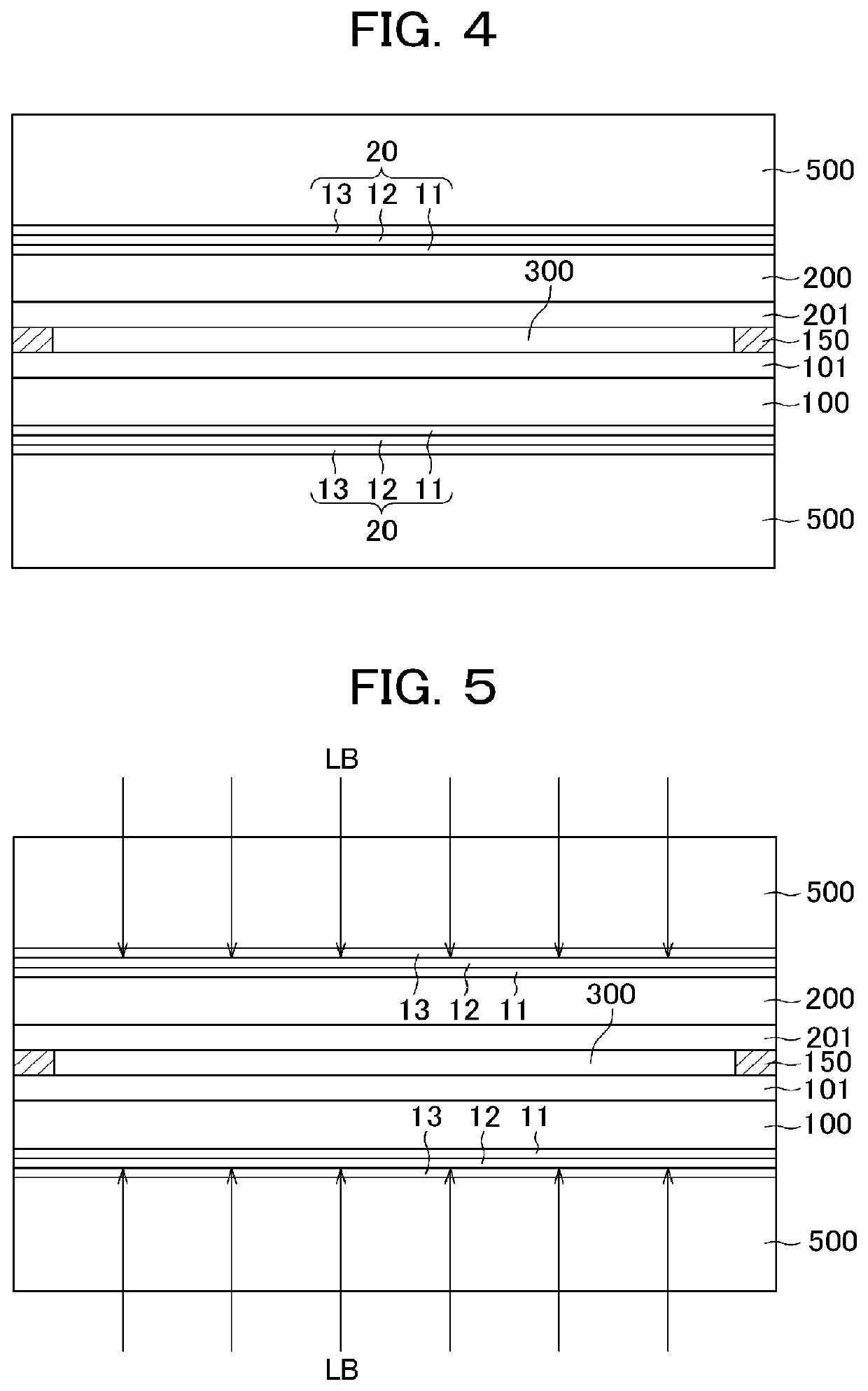
[0084]FIG. 15 is a cross sectional view of embodiment 3 according to the present invention. FIG. 15 differs from FIG. 8 of embodiment 1 in that the a-Si layer 12 and the glass substrate 500 directly contact each other in FIG. 15. The adhesive strength between the a-Si layer 12 and glass substrate 500 is less than the adhesive strength between the glass substrate 500 and the nitride layer such as the SiN layer, the TiN layer, or the AlO layer; however, it still has enough adhesive strength to enable the assembly of the glass substrate 500 and the polyimide substrate 100 to go through stably in the manufacturing process. A thickness of the a-Si layer 12 in FIG. 15 is e.g. 50 to 100 nm, which is a little bit thicker than the thickness of the a-Si layer 12 in FIG. 11 and so forth.
[0085]FIG. 16 is a cross sectional view depicting a state in which the a-Si layer 12 in the structure of FIG. 15 is irradiated with the excimer laser LB for laser ablation. In FIG. 16, when the a-Si layer 12 is...
PUM
 Abstract
Description
Claims
Application Information
 - R&D
- Intellectual Property
- Life Sciences
- Materials
- Tech Scout
- Unparalleled Data Quality
- Higher Quality Content
- 60% Fewer Hallucinations
Browse by: Latest US Patents, China's latest patents, Technical Efficacy Thesaurus, Application Domain, Technology Topic, Popular Technical Reports.
© 2025 PatSnap. All rights reserved.Legal|Privacy policy|Modern Slavery Act Transparency Statement|Sitemap|About US| Contact US: help@patsnap.com