Barrier film for electronic devices
- Summary
- Abstract
- Description
- Claims
- Application Information
AI Technical Summary
Benefits of technology
Problems solved by technology
Method used
Image

Examples
Embodiment Construction
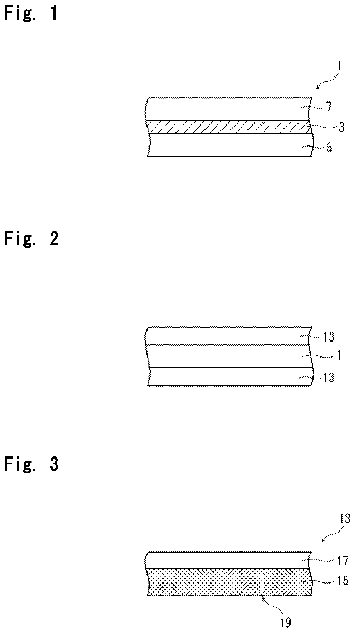
[0026]The barrier film of the present invention has a water permeability (23° C., RH50%) that is set to be not more than 10−4 g / m2 / day, more preferably, not more than 10−5 g / m2 / day and, most preferably, not more than 10−6 g / m2 / day, and a water content that is maintained to be not more than 2000 ppm and, specifically, not more than 100 ppm. By overlapping a plurality of the inorganic barrier layers one upon the other or by being fabricated in a multilayered structure including a water-trapping layer that absorbs and traps the water, the barrier film of the present invention having such a low water permeability and a small water content becomes capable of improving the barrier property against oxygen or against the water and hence becomes capable of exhibiting improved performance as a sealing member for a variety of kinds of devices.
[0027]FIG. 1 illustrates a structure of layers of such a barrier film.
[0028]Referring to FIG. 1, the barrier film of the present invention generally desi...
PUM
| Property | Measurement | Unit |
|---|---|---|
| Temperature | aaaaa | aaaaa |
| Fraction | aaaaa | aaaaa |
| Fraction | aaaaa | aaaaa |
Abstract
Description
Claims
Application Information
 - R&D
- Intellectual Property
- Life Sciences
- Materials
- Tech Scout
- Unparalleled Data Quality
- Higher Quality Content
- 60% Fewer Hallucinations
Browse by: Latest US Patents, China's latest patents, Technical Efficacy Thesaurus, Application Domain, Technology Topic, Popular Technical Reports.
© 2025 PatSnap. All rights reserved.Legal|Privacy policy|Modern Slavery Act Transparency Statement|Sitemap|About US| Contact US: help@patsnap.com