
Distributed bragg reflector structures in multijunction solar cells

a solar cell and reflector technology, applied in the direction of sustainable manufacturing/processing, climate sustainability, semiconductor devices, etc., can solve the problems of reducing current, increasing the complexity of properly specifying and manufacturing, and reducing power output, so as to increase the photoconversion efficiency

Inactive Publication Date: 2020-08-06
SOLAERO TECH CORP
View PDF0 Cites 13 Cited by
  • Summary
  • Abstract
  • Description
  • Claims
  • Application Information

AI Technical Summary

Benefits of technology

[0012]It is an object of the present disclosure to provide increased photoconversion efficiency in a multijunction solar cell for space applications by incorporating a plurality of distributed Bragg reflector structures between two adjacent subcells in the multijunction solar cell.
[0037]In some embodiments, the difference in refractive indices between alternating layers is maximized in order to minimize the number of periods required to achieve a given reflectivity, and the thickness and refractive index of each period determines the stop band and its limiting wavelength.

Problems solved by technology

Compared to silicon, III-V compound semiconductor multijunction devices have greater energy conversion efficiencies and generally more radiation resistance, although they tend to be more complex to properly specify and manufacture.
However, in reality, changing a material parameter that increases the voltage may result in a decrease in current, and therefore a lower power output.
Such material design parameters are interdependent and interact in complex and often unpredictable ways, and for that reason are not “result effective” variables that those skilled in the art confronted with complex design specifications and practical operational considerations can easily adjust to optimize performance.

Method used


Image

  • Distributed bragg reflector structures in multijunction solar cells
  • Distributed bragg reflector structures in multijunction solar cells
  • Distributed bragg reflector structures in multijunction solar cells

Examples


Embodiment Construction

[0082]Details of the present invention will now be described including exemplary aspects and embodiments thereof. Referring to the drawings and the following description, like reference numbers are used to identify like or functionally similar elements, and are intended to illustrate major features of exemplary embodiments in a highly simplified diagrammatic manner. Moreover, the drawings are not intended to depict every feature of the actual embodiment nor the relative dimensions of the depicted elements, and are not drawn to scale.

[0083]A variety of different features of multijunction solar cells (as well as inverted metamorphic multijunction solar cells) are disclosed in the related applications noted above. Some, many or all of such features may be included in the structures and processes associated with the lattice matched or “upright” solar cells of the present disclosure. However, more particularly, the present disclosure is directed to the fabrication of a multijunction latt...


PUM

PropertyMeasurementUnit
spectral wavelength rangeaaaaaaaaaa
band gapaaaaaaaaaa
band gapaaaaaaaaaa

Abstract

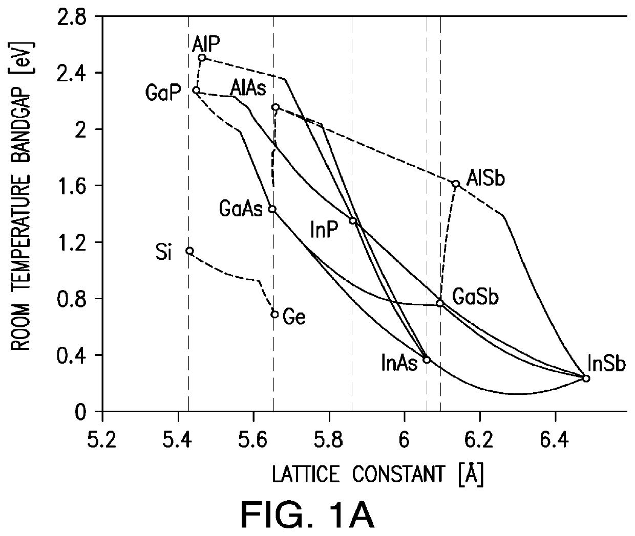
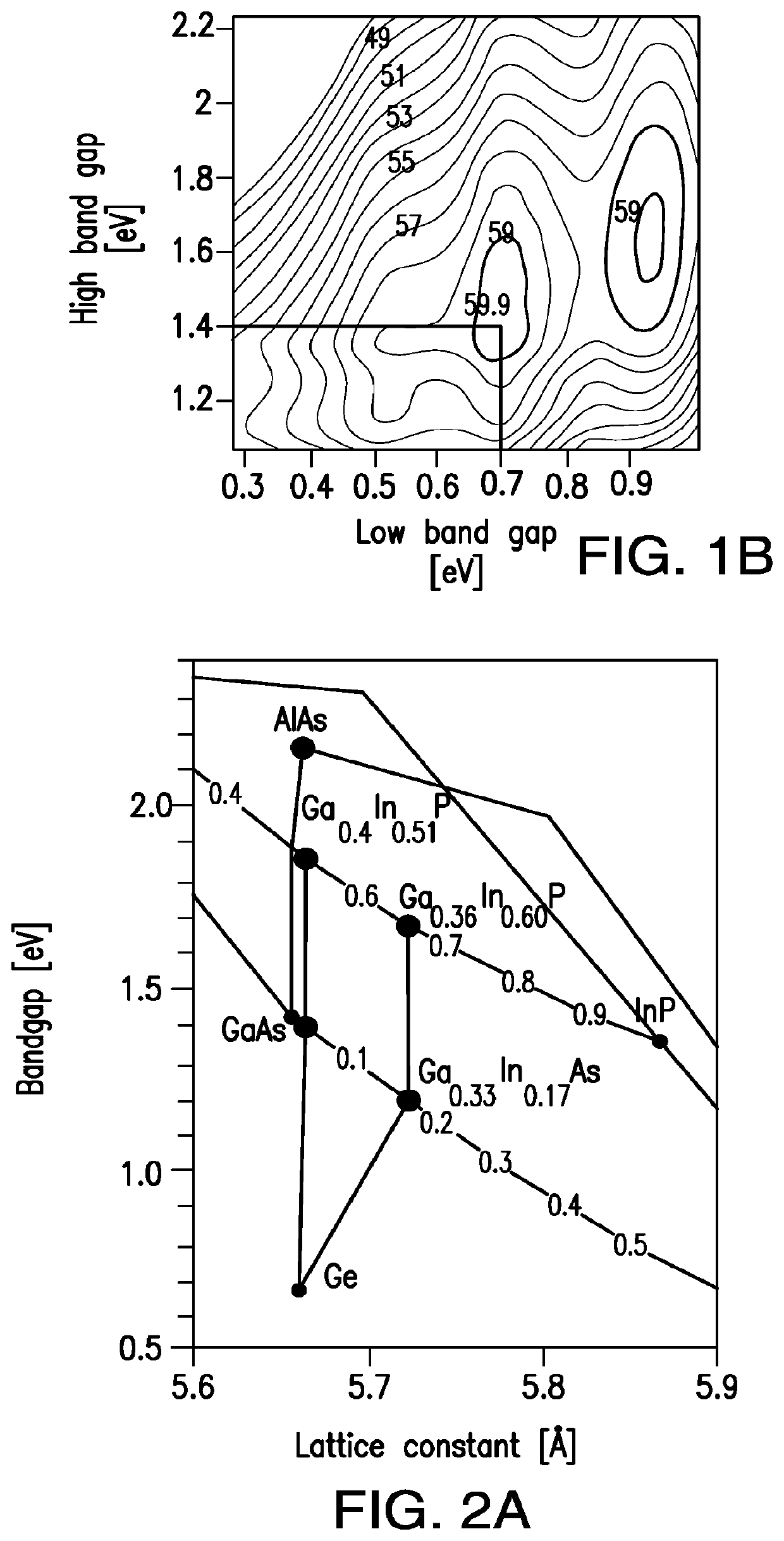
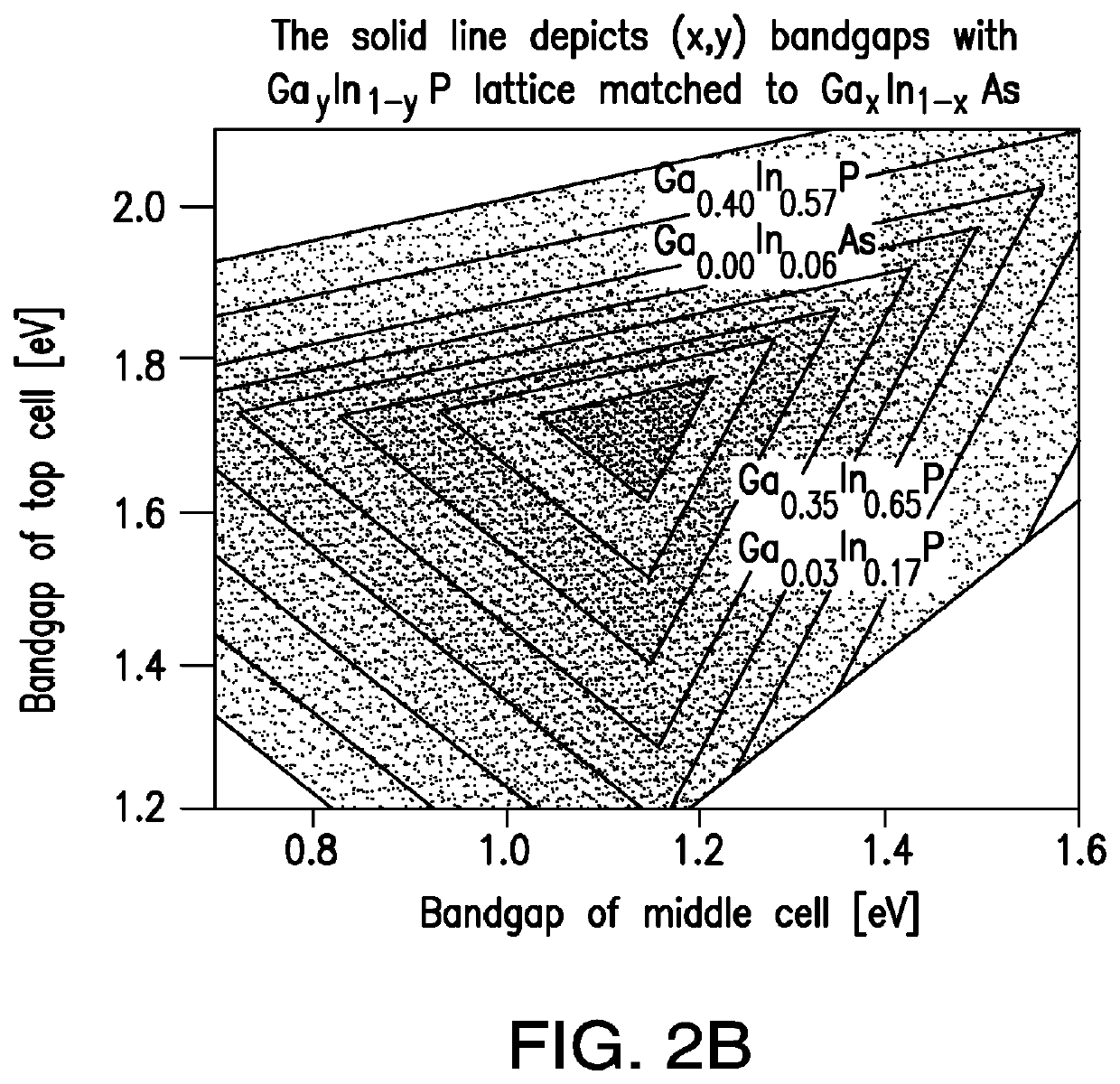
A multijunction solar cell and its method of fabrication, having an upper first solar subcell composed of a semiconductor material including aluminum and having a first band gap; a second solar subcell adjacent to said first solar subcell and composed of a semiconductor material having a second band gap smaller than the first band gap and being lattice matched with the upper first solar subcell; a third solar subcell adjacent to said second solar subcell and composed of a semiconductor material having a third band gap smaller than the second band gap and being lattice matched with the second solar subcell; a first and second DBR structure adjacent to the third solar subcell; and a fourth solar subcell adjacent to the DBR structures and lattice matched with said third solar subcell and composed of a semiconductor material having a fourth band gap smaller than the third band gap; wherein the fourth subcell has a direct bandgap of greater than 0.75 eV.

Description

REFERENCE TO RELATED APPLICATIONS[0001]This application is a continuation of U.S. patent application Ser. No. 15 / 376,195 filed Dec. 12, 2016.[0002]This application is related to co-pending U.S. patent application Ser. No. 14 / 660,092 filed Mar. 17, 2015, which is a division of U.S. patent application Ser. No. 12 / 716,814 filed Mar. 3, 2010, now U.S. Pat. No. 9,018,521; which was a continuation in part of U.S. patent application Ser. No. 12 / 337,043 filed Dec. 17, 2008.[0003]This application is also related to co-pending U.S. patent application Ser. No. 13 / 872,663 filed Apr. 29, 2013, now U.S. Pat. No. 10,541,349 which was also a continuation-in-part of application Ser. No. 12 / 337,043, filed Dec. 17, 2008.[0004]This application is also related to U.S. patent application Ser. No. 14 / 828,197, filed Aug. 17, 2015.[0005]All of the above related applications are incorporated herein by reference in their entirety.BACKGROUND OF THE INVENTIONField of the Invention[0006]The present disclosure re...

Claims


Application Information

Patent Timeline
Patent Type & Authority Applications(United States)
IPC IPC(8): H01L31/054H01L31/0687H01L31/0216H01L31/0232H01L31/18H01L31/0304H01L31/0693
CPCH01L31/0693H01L31/0687H01L31/1844H01L31/03046Y02E10/50H01L31/0216H01L31/02168H01L31/0549H01L31/02167H01L31/06875H01L31/02327Y02E10/544H01L31/078H01L31/056H01L31/035236Y02E10/52Y02P70/50
Inventor MCGLYNN, DANIELDERKACS, DANIEL
Owner SOLAERO TECH CORP
Learn More