Resonant cavity enhanced image sensor

a resonance cavity and image sensor technology, applied in the field of image sensors, can solve the problems of limiting the sharpness of the image, difficult to detect near infrared light with silicon photodiodes, and inability to thicken the detector layer, so as to reduce the depth of the region and high quantum efficiency

Active Publication Date: 2020-06-18
AMS AG
View PDF0 Cites 3 Cited by
  • Summary
  • Abstract
  • Description
  • Claims
  • Application Information

AI Technical Summary

Benefits of technology

[0011]The resonant cavity enhanced image sensor makes use of a resonating optical cavity. It provides high quantum efficiency and a reduced depth of the region where charge carriers are generated and detected. This image sensor can be realized as a CMOS image sensor and applied in conjunction with infrared light sources, which may be tuned typically to a wavelength of 940 nm, for example. The concept can also be employed to CCDs (charge-coupled devices).

Problems solved by technology

Near infrared light is difficult to detect with silicon photodiodes as commonly used in CMOS and CCD image sensors.
A thick detector layer is not feasible in an array of small pixels each containing a photodiode, because crosstalk between pixels caused by carrier diffusion would limit the sharpness of the image.
Such backside bias technique also requires additional process steps in manufacturing, increasing cost of the device.
Thicker detector layers also limit the maximum speed at which charge carriers can be collected.
In case when the optical path length between the mirrors is a multiple of the wavelength of the light in the material inside the cavity, a constructive interference occurs.

Method used


Image

  • Resonant cavity enhanced image sensor
  • Resonant cavity enhanced image sensor
  • Resonant cavity enhanced image sensor

Examples


Embodiment Construction

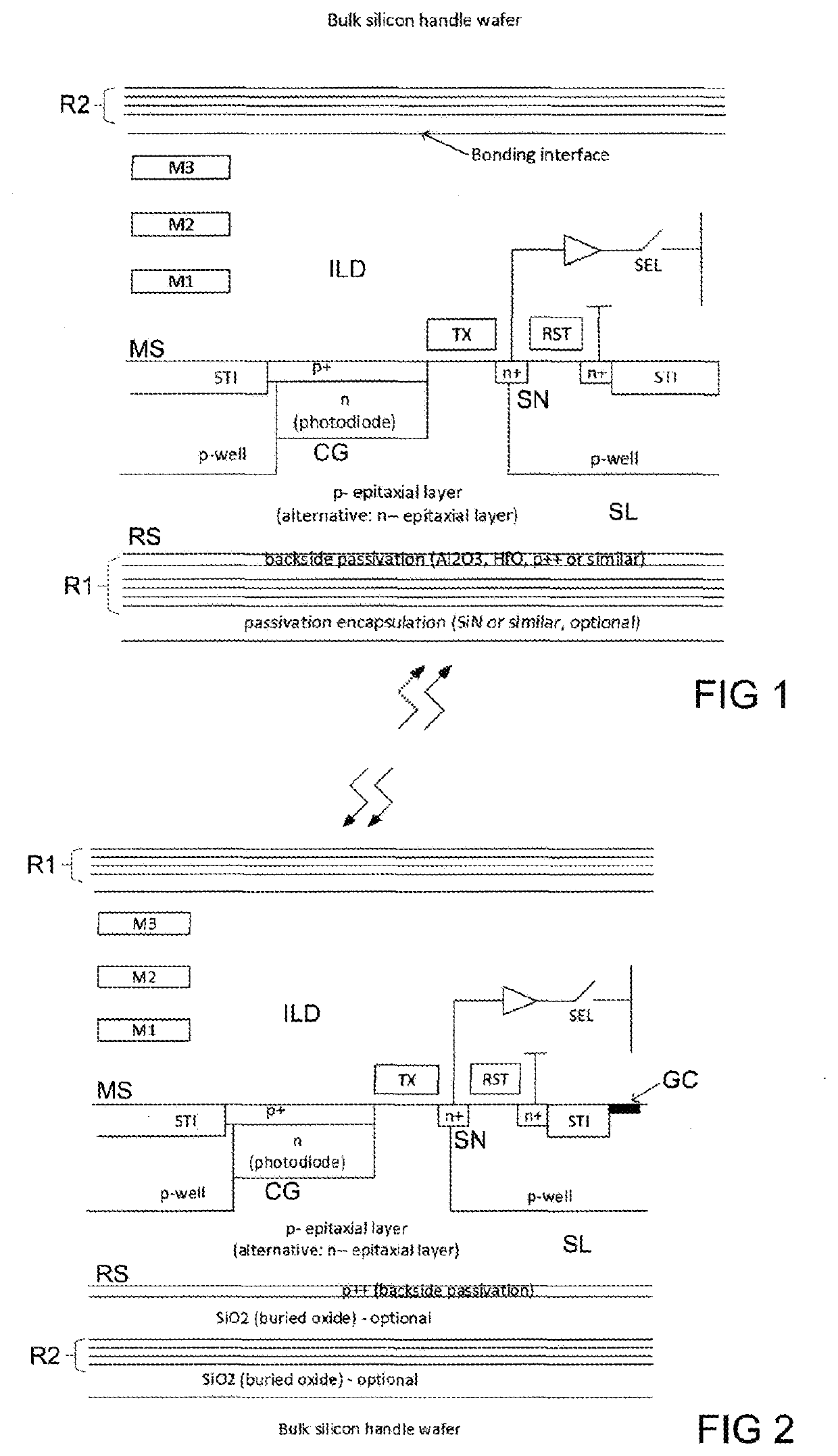
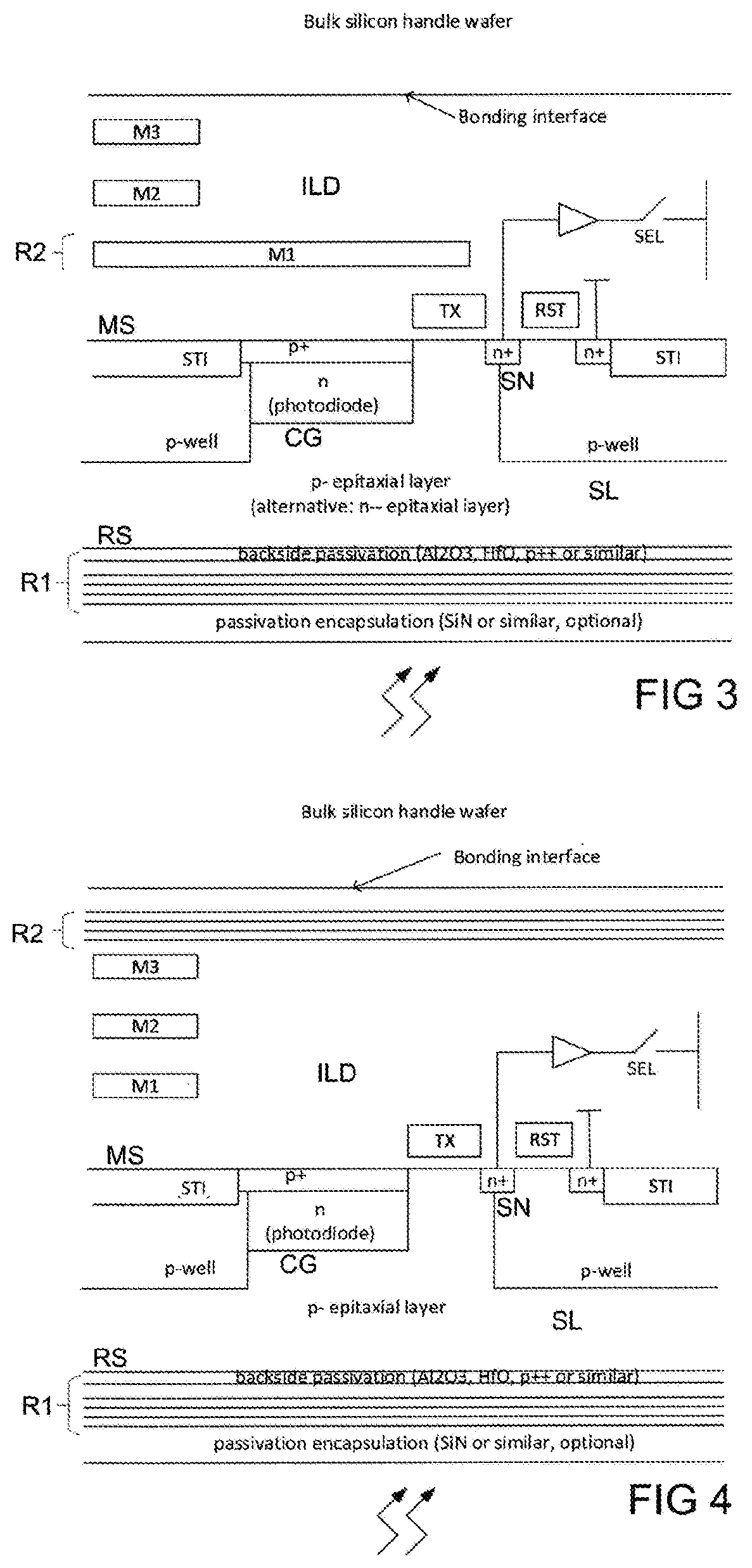
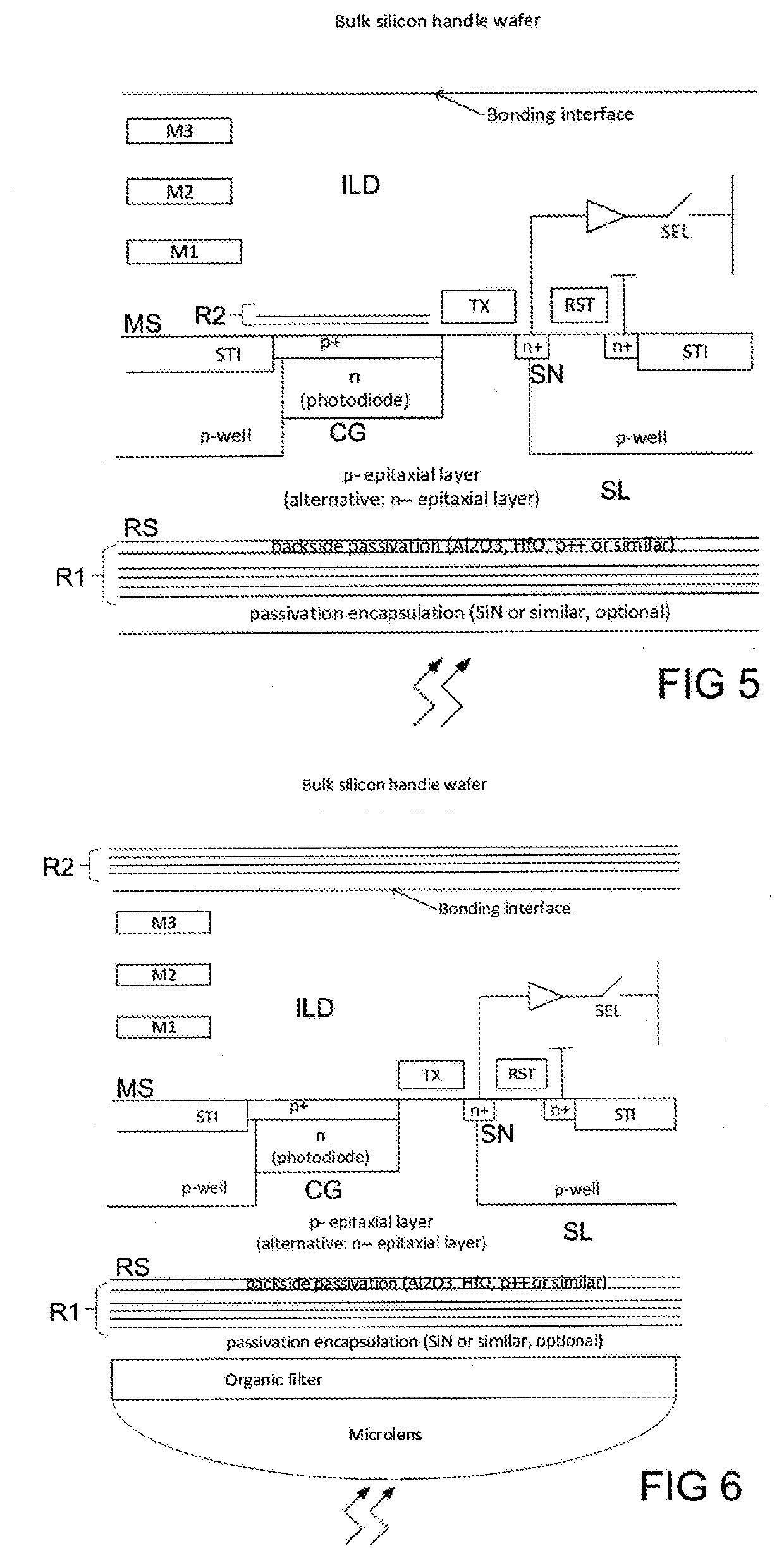
[0045]In the following description, the charge carrier generating component CG is represented by a photodiode, by way of example. The charge carriers may be transferred to a sense node SN through a transfer gate TX.

[0046]FIG. 1 shows a back-illuminated image sensor, which may be a CMOS image sensor. Light enters from the rear side RS of the semiconductor layer SL, which may be silicon, for instance. The semiconductor layer SL may especially be an epitaxial layer of p-type or n-type conductivity. The reflecting layers R1, R2 are arranged above the rear side RS as a top mirror or top reflecting layer R1 and above the active part of the image sensor, which is represented by a photodiode, as a bottom mirror or bottom reflecting layer R2. The reflecting layers R1, R2 form opposite boundaries of a resonant cavity. The distance between the reflecting layers R1, R2 is tuned to obtain a desired resonance. The reflectance may typically be tuned to 940 nm, for example.

[0047]Inside the cavity t...


PUM

PropertyMeasurementUnit
wavelengthaaaaaaaaaa
absorption depthaaaaaaaaaa

Abstract

The semiconductor image sensor device comprises a semiconductor layer having a main surface and an opposite rear surface, and a charge carrier generating component at the main surface. The charge carrier generating component is arranged between a top reflecting layer and a bottom reflecting layer, which are arranged outside the semiconductor layer.

Description

BACKGROUND OF THE INVENTION[0001]This disclosure concerns the field of image sensors, in particular image sensors to be optimized for a good quantum efficiency at a specific wavelength. Such image sensors are used, for example, in systems where artificial light is projected, like a camera system using a structured light pattern for 3D imaging or a system using a set of short light pulses such as used in time-of-flight 3D imaging systems. Such systems often use narrowband near infrared light because near infrared light is not visible to the user. Near infrared light is difficult to detect with silicon photodiodes as commonly used in CMOS and CCD image sensors. But particular bands in the infrared region are interesting because of their low sunlight content, e.g. the H2O absorption band around 940 nm, which means that there is significantly less background signal in an actively illuminated system. It is then advantageous to use a narrowband 940 nm light source so that the amount of ba...

Claims


Application Information

Patent Timeline
Patent Type & Authority Applications(United States)
IPC IPC(8): H01L27/146
CPCH01L27/14636H01L27/14649H01L27/1462H01L27/14629H01L27/1464H01L27/14685H01L27/14643H01L27/14665
Inventor MEYNANTS, GUY
Owner AMS AG
Why Eureka
Try Eureka