An optoelectronic apparatus, a method for suppressing noise for an optoelectronic apparatus, and uses thereof
a technology of optoelectronic equipment and optoelectronic device, which is applied in the field of optoelectronic device, can solve the problems of increasing the cost and size of the final product, unable to detect the low level of light level, and high noise equivalent irradiance, so as to reduce the noise equivalent irradiance or noise equivalent power, and the effect of low light level
- Summary
- Abstract
- Description
- Claims
- Application Information
AI Technical Summary
Benefits of technology
Problems solved by technology
Method used
Image
Examples
embodiment 1
hutter Implemented Via Bottom Gate and Top Contact Modulation
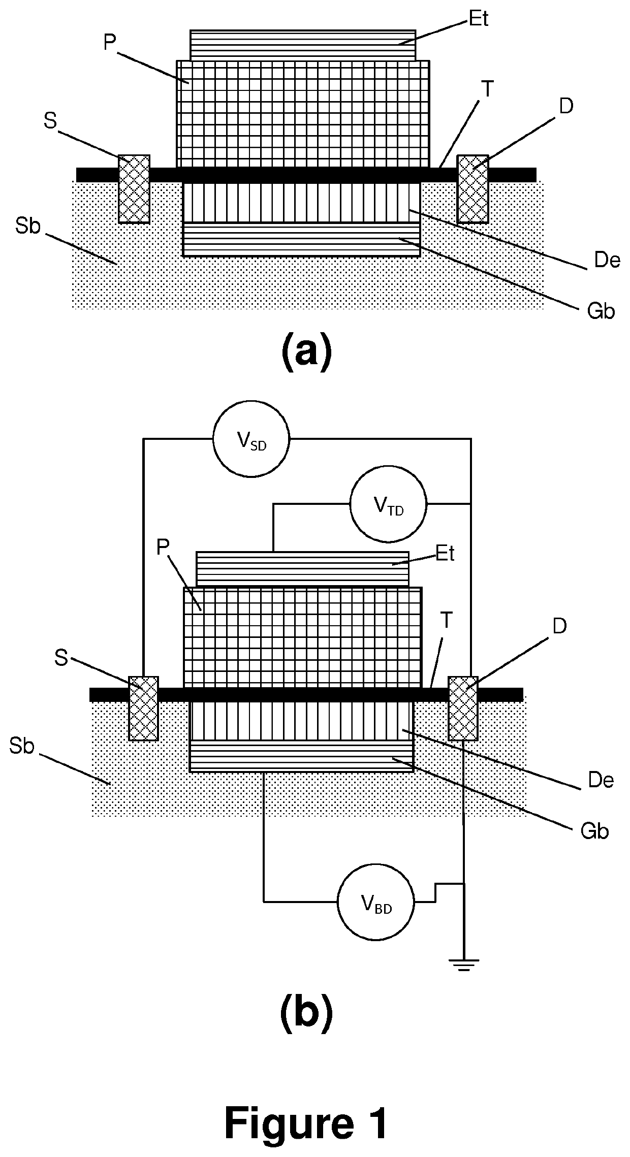
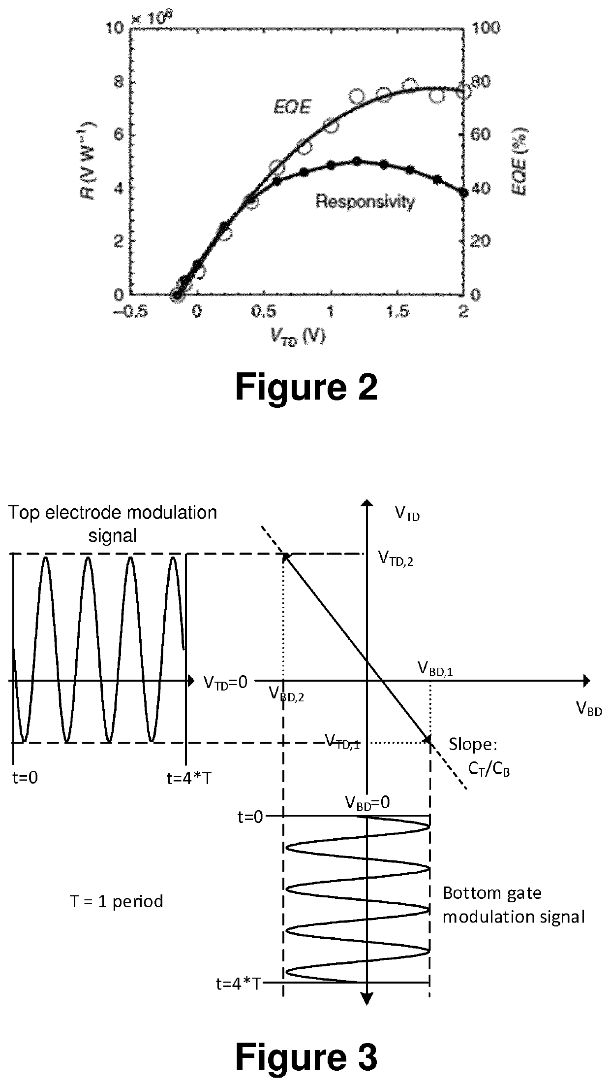
[0109]For this embodiment, the optoelectronic device of the optoelectronic apparatus of the first aspect of the present invention has the arrangement depicted by FIG. 1(a), i.e. a substrate Sb, and arranged thereon:[0110]a conductive bottom gate electrode structure Gb;[0111]a dielectric structure / layer De arranged over the conductive bottom gate electrode structure Gb;[0112]a transport structure T comprising one or more 2-dimensional layers arranged over the dielectric structure De;[0113]a photosensitizing structure / layer P (semiconducting light absorber) and arranged over the transport structure T and configured and arranged to absorb incident light and induce changes in the electrical conductivity of the transport structure T;[0114]a top electrode Et electrically connected (ohmic contact or Schottky contact) to the photosensitizing structure P; and[0115]drain D and source S electrodes electrically connected to respective...
embodiment 2
hutter Implemented Via Bottom Pate and Top Pate Modulation
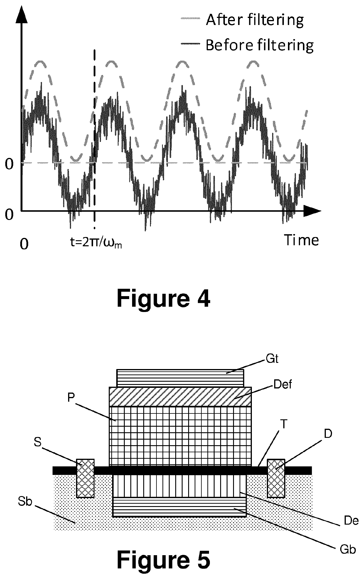
[0135]For this embodiment 2, the optoelectronic device of the optoelectronic apparatus of the first aspect of the present invention has the arrangement depicted by FIG. 5, i.e. one which differs from the one of FIG. 1 in that, instead of including a top electrode, it includes a top gate Gt isolated from the photosensitizing structure P by a further dielectric structure Def.
[0136]The optoelectronic apparatus of Embodiment 2 includes the device of FIG. 5 and an electronic connection scheme as illustrated in FIG. 1(b), i.e. including voltage generators VBD, VTD, and VSD of the control unit (not shown) included in the modulation unit of the noise suppression means of the present invention, but where the voltage generator VTD is connected to the top gate Gt (instead of to a top electrode Et).
[0137]On the same grounds as described in Embodiment 1, modulation is implemented using respective oscillating signals (voltage oscillation s...
embodiment 3
ssion Using Bottom Date Modulation
[0142]For this embodiment, the optoelectronic device of the optoelectronic apparatus of the first aspect of the present invention has the arrangement depicted by FIG. 6, i.e. a substrate Sb, and arranged thereon:[0143]a conductive bottom gate electrode structure Gb;[0144]a dielectric structure / layer De arranged over the conductive bottom gate electrode structure Gb;[0145]a transport structure T comprising one or more 2-dimensional graphene layers arranged over the dielectric structure De;[0146]a photosensitizing structure / layer P (semiconducting light absorber) arranged over the transport structure T and configured and arranged to absorb incident light and induce changes in the electrical conductivity of the transport structure T; and[0147]drain D and source S electrodes electrically connected to respective separate locations of the transport structure T.
[0148]In this case, the present invention benefits specifically from the ambipolar conduction na...
PUM
 Abstract
Description
Claims
Application Information
 - R&D
- Intellectual Property
- Life Sciences
- Materials
- Tech Scout
- Unparalleled Data Quality
- Higher Quality Content
- 60% Fewer Hallucinations
Browse by: Latest US Patents, China's latest patents, Technical Efficacy Thesaurus, Application Domain, Technology Topic, Popular Technical Reports.
© 2025 PatSnap. All rights reserved.Legal|Privacy policy|Modern Slavery Act Transparency Statement|Sitemap|About US| Contact US: help@patsnap.com


