Ballistic field-effect transistors based on bloch resonance and methods of operating a transistor

a field-effect transistor and bloch resonance technology, applied in the field of field-effect transistors, can solve the problems of reducing the effectiveness of the mosfet, unable to function properly, and continuing advancemen

Active Publication Date: 2020-04-23
THE RES FOUND OF STATE UNIV OF NEW YORK
View PDF0 Cites 2 Cited by
  • Summary
  • Abstract
  • Description
  • Claims
  • Application Information

AI Technical Summary

Benefits of technology

[0017]FIG. 2 is a top view diagram of a ballistic Bloch-Field Effect Transistor (BBFET) gate-channel configuration according to an embodiment of the present disclosure, wherein the transistor is shown in the volatile OFF state. The gate-arms are electrically connected and connected to negative potential on the source;

Problems solved by technology

1) As shown in FIG. 1A, a basic MOSFET structure includes two types of semiconductor—n-type and p-type—and their junctions (shown in FIG. 1A as a depletion region). When dimensions of transistors go to the submicron scale, the p-n junctions begin to operate as part of parasitic junction transistors because a potential applied to the gate affects the whole MOSFET structure. As a result, the bias potential drives the parasitic transistors and this phenomenon dramatically reduces MOSFET effectiveness.
2) Another weak feature of the basic structure is a thin dielectric layer (oxide), located between the gate and the channel. The presence of this thin oxide layer sets a lower limit to the transistor size and this constraint will end eventually Moore's law.
This will result in the failure of the transistor to function properly.
3) Another drawback of the basic MOSFET configuration that fundamentally prevents continued advancement is the principal of MOSFET operation itself.
However, the performance of these transistors was significantly lower (low currents) compared to MOSFET transistors or HEMTs.

Method used


Image

  • Ballistic field-effect transistors based on bloch resonance and methods of operating a transistor
  • Ballistic field-effect transistors based on bloch resonance and methods of operating a transistor
  • Ballistic field-effect transistors based on bloch resonance and methods of operating a transistor

Examples


Embodiment Construction

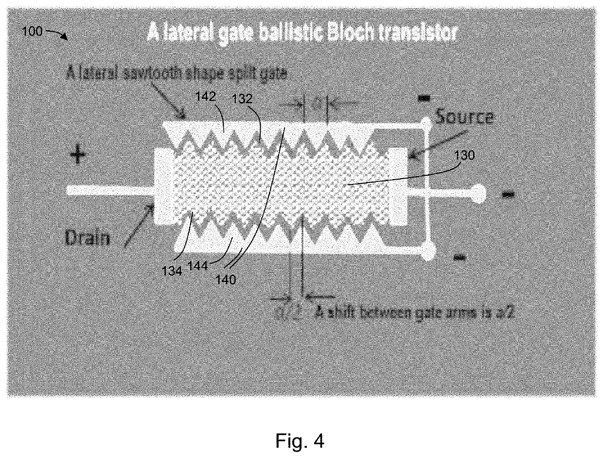
[0039]In a first aspect, the present disclosure may be embodied as a semiconductor device 10 (a lateral-gate ballistic Bloch field-effect transistor or “BBFET”) having a source 22 and a drain 24 spaced apart from the source 22 (see, e.g., FIG. 2). The source 22 and the drain 24 may be fabricated using known Ohmic technology. In some embodiments, the structure may be disposed on a substrate 12. A channel 30 is electrically connected to the source 22 and the drain 24. The channel 30 may be a two-dimensional conducting layer (2DCL), such as, for example, a two-dimensional electron gas (2DEG). The channel 30 has a length (i.e., a channel length) measured from the source 22 to the drain 24. The channel length (L) is selected to be less than or equal to an electron mean free path of the material from which the channel is made (as further described below). In this way, the channel 30 has a ballistic electron transport-resulting in the BBFET as a ballistic transistor. Depending on channel ...


PUM

PropertyMeasurementUnit
Fermi levelaaaaaaaaaa
current oscillationsaaaaaaaaaa

Abstract

A semiconductor device includes a source, a drain, and a channel electrically connected to the source and the drain. The channel has a channel length from the drain to the source which is less than or equal to an electron mean free path of the channel material. A first gate has two arms, each extending between the drain and the source (i.e., at least a portion of the distance between the source and the drain). Each arm of the first gate is disposed proximate to a corresponding first and second edge of the channel. Each arm of the first gate has a periodic profile along an inner boundary, wherein the periodic profiles of each arm are offset from each other such that a distance between the arms is constant. A Bloch voltage applied to the first gate will reduce the effective channel with such that Bloch resonance conditions are met.

Description

CROSS-REFERENCE TO RELATED APPLICATIONS[0001]This application claims priority to U.S. Provisional Application No. 62 / 747,106, filed on Oct. 17, 2018, now pending, the disclosure of which is incorporated herein by reference.FIELD OF THE DISCLOSURE[0002]The present disclosure relates to transistors, and more particularly to field-effect transistors.BACKGROUND OF THE DISCLOSURE[0003]On average, 8 trillion transistors are produced every second. In 2014 (50 years of Moore's law), semiconductor production facilities made some 250 billion billion (250×1018) transistors. IEEE Spectrum magazine called this transistor production at “astronomical scales.”[0004]In 1958-1960, Dawon Kahng and Martin Atalla (Bell Labs) invented the metal-oxide semiconductor field-effect transistor (MOSFET), and in 1963, the invention issued as U.S. Pat. No. 3,102,230. A typical MOSFET structure is shown in FIG. 1A. However, MOSFETs have several major drawbacks which have slowed development in transistor technology...

Claims


Application Information

Patent Timeline
Patent Type & Authority Applications(United States)
IPC IPC(8): H01L29/778H03B1/02H01L29/10
CPCH03B1/02H01L29/1029H01L29/7786H01L29/1606H01L29/2003H01L29/24H01L29/42356H01L29/4238H01L29/778H03B28/00
Inventor POGREBNYAK, VICTORBIRD, JONATHAN
Owner THE RES FOUND OF STATE UNIV OF NEW YORK
Why Eureka
Try Eureka