Input device

a technology of input device and air bubble, which is applied in the direction of printed circuit manufacturing, instruments, printed circuit assembling, etc., can solve the problems of air bubble interference, poor appearance, and invite an increase in the number of manufacturing steps, and achieve the effect of narrowing the length of a region, reducing the number of manufacturing steps, and increasing the thickness of the protection layer

Active Publication Date: 2020-03-05
ALPS ALPINE CO LTD
View PDF0 Cites 1 Cited by
  • Summary
  • Abstract
  • Description
  • Claims
  • Application Information

AI Technical Summary

Benefits of technology

[0013]According to this configuration, a step of the optical layer can be absorbed from the protruding part of the flexible base member toward the sensing region side in the part into which the conductive joining member does not stick out. This makes it possible to narrow a length of a region where an air bubble formed by the step of the optical layer is present.
[0014]The input device may be configured such that a height, from the first surface, of the conductive joining member that sticks out toward the sensing region side beyond the protruding part is equal to or lower than a height of the protruding part from the first surface. This makes it possible to absorb the step of the optical layer from the front end of the protruding part toward the sensing region side even in a case where a part of the conductive joining member protrudes beyond the protruding part of the flexible base member.
[0015]The input device may be configured to further include a protection layer provided between the light-transmitting electrode unit and the optical layer, wherein an adhesive layer that fixes the protection layer and the optical layer is located so as to reach an end of an outer periphery of a main surface of the protection layer. With this configuration, the air bubble is located on an outer side of the protection layer, and therefore a length of the air bubble region can be narrowed.
[0016]The input device may be configured such that a ratio of a thickness of the protection layer to the height of the protruding part from the first surface is 0.2 or more. A larger thickness of the protection layer leads to a smaller step of the optical layer and is therefore more preferable. That is, only from the perspective of reduction of the step, the ratio closer to 1 is more preferable, and as a result, the larger thickness of the protection layer is more preferable. However, a too large thickness of the protection layer decreases flexibility of the input device (touch panel). In view of this, the thickness of the protection layer is realistically approximately 15 μm at most and is preferably 10 μm or less.

Problems solved by technology

This air bubble interferes depending on an optical angle and deforms the optical layer by expanding in volume under a high-temperature environment.
This can be a cause of poor appearance.
However, this requires a step of injecting the resin, thereby inviting an increase in the number of manufacturing steps.
In such cases, however, a large buffer region is needed in a case where the region where the air bubble is located is large.
It is therefore difficult to meet recent demands for narrowing of a width of a region (where a draw-out wire is disposed) around the detection region.

Method used


Image

  • Input device
  • Input device
  • Input device

Examples


Embodiment Construction

[0030]An embodiment of the present invention is described below with reference to the drawings. In the following description, identical members are given identical reference signs, and description of members described once is omitted as appropriate.

Configuration of Input Device

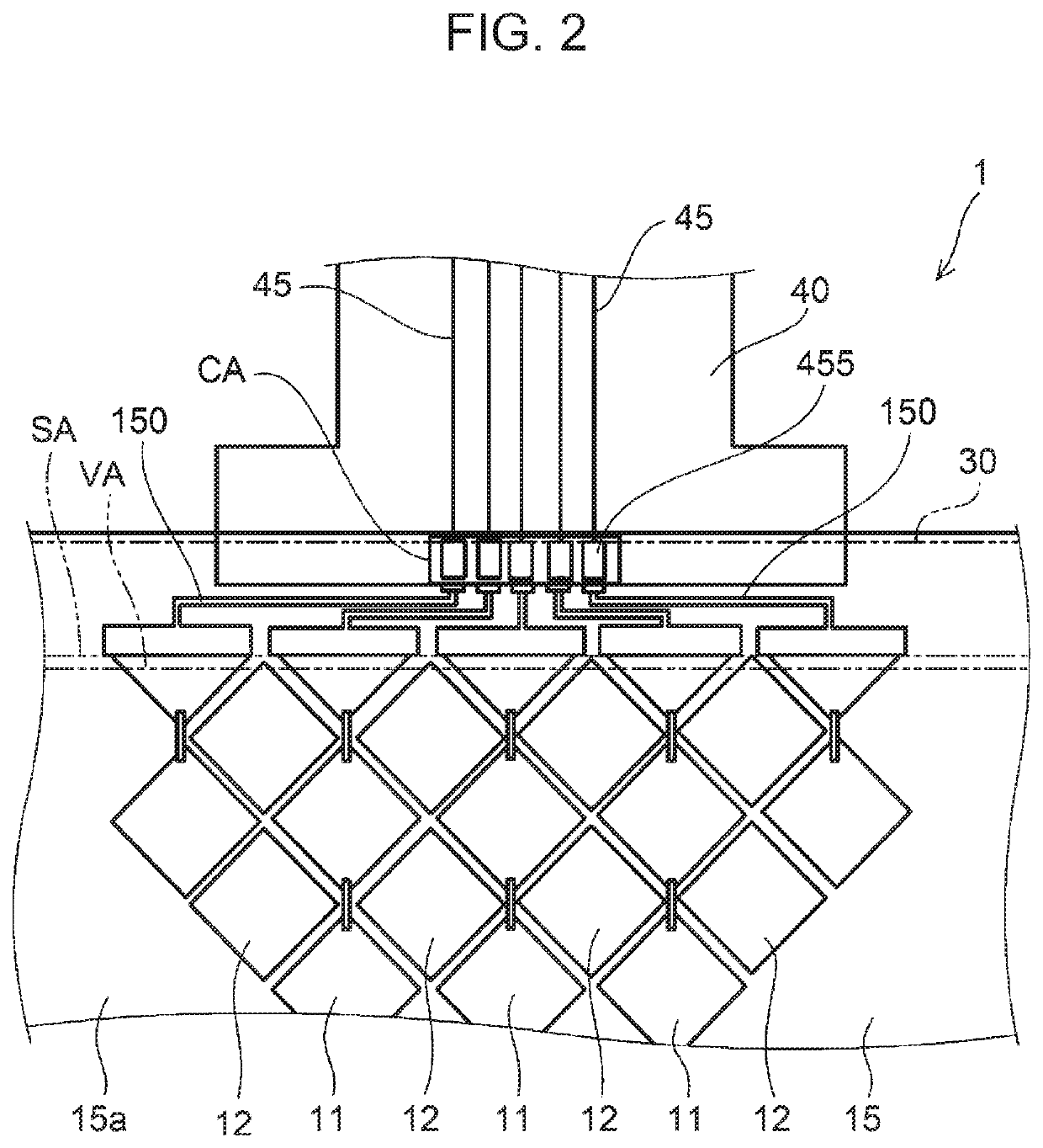
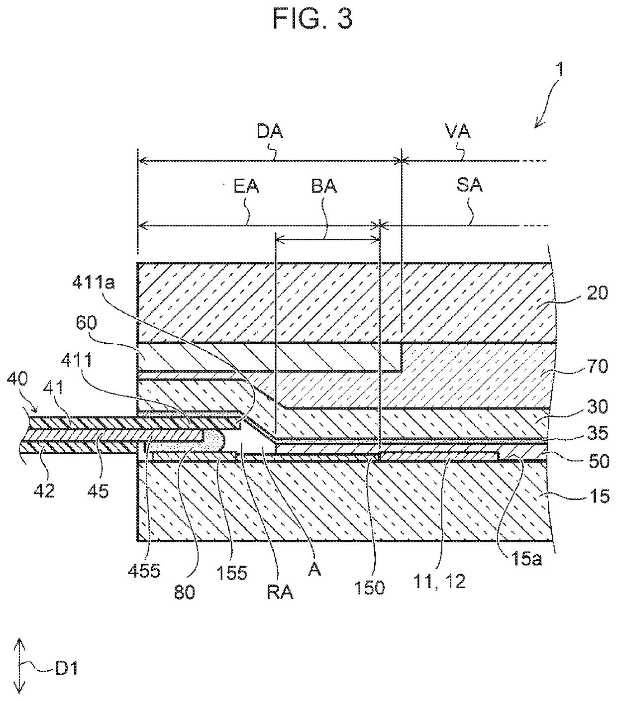
[0031]FIG. 1 is an exploded perspective view illustrating an input device according to the present embodiment. FIG. 2 is a plan view schematically illustrating the input device according to the present embodiment. More specifically, FIG. 2 is a plan view schematically illustrating a connection part of a flexible wiring substrate 40 in the input device 1. FIG. 3 is a cross-sectional view schematically illustrating the input device according to the present embodiment. More specifically, FIG. 3 is a cross-sectional view schematically illustrating the connection part of the flexible wiring substrate 40 in the input device 1. For convenience of description, a display device 100 is not illustrated in FIG. 3.

[0032]As...


PUM

PropertyMeasurementUnit
thicknessaaaaaaaaaa
thicknessaaaaaaaaaa
thicknessaaaaaaaaaa

Abstract

An input device includes a sensor unit, an optical layer superimposed on the sensor unit, and a flexible wiring substrate having a connection region held between the optical layer and support base member. The flexible wiring substrate has a flexible base member on which an electrode layer is provided and a wiring end that is an end of the electrode layer and is conductive with the terminal part with a conductive joining member. The wiring end is set back from an end of the flexible base member, so that the flexible base member has a protruding part protruding toward the sensing region. Since the input device has, on the sensing region side relative to a front end of the protruding part, a part into which the conductive joining member does not stick out, an air bubble region between the sensor unit and the optical layer can be narrowed.

Description

CLAIM OF PRIORITY[0001]This application is a Continuation of International Application No. PCT / JP2018 / 019937 filed on May 24, 2018, which claims benefit of Japanese Patent Application No. 2017-127174 filed on Jun. 29, 2017. The entire contents of each application noted above are hereby incorporated by reference.BACKGROUND OF THE INVENTION1. Field of the Invention[0002]The present invention relates to an input device. More specifically, the present invention relates to an input device including a touch sensor that detects a position of approach of a finger or the like.2. Description of the Related Art[0003]A touch panel often used as an input device includes a touch sensor that detects a position of approach (hereinafter, approach encompasses contact) of a finger or the like to a detection region. For example, a mutual capacitance touch panel is provided with a drive-side electrode and an output-side electrode. The drive-side electrode is given a drive pulse, and the output-side elec...

Claims


Application Information

Patent Timeline
Patent Type & Authority Applications(United States)
IPC IPC(8): G06F3/047H05K3/32H05K3/36G06F3/044
CPCH05K3/323H05K3/361G06F3/047G06F2203/04102G06F3/044G06F1/1643G06F3/04164H05K1/118G06F3/0446G06F2203/04103H05K1/147
Inventor MOTONISHI, MICHIHARUKOBAYASHI, KIYOSHI
Owner ALPS ALPINE CO LTD
Why Eureka
Try Eureka