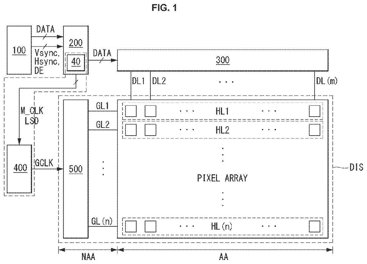
Gate clock generator and display device having the same
a display device and generator technology, applied in the direction of instruments, static indicating devices, etc., can solve the problems of limitation of gate pulses applied to the lines of display panels, same phase and same pulse width
- Summary
- Abstract
- Description
- Claims
- Application Information
AI Technical Summary
Benefits of technology
Problems solved by technology
Method used
Image
Examples
first embodiment
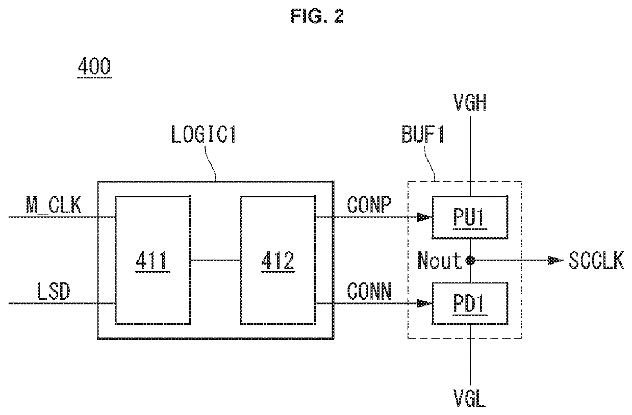
[0045]Referring to FIGS. 2 to 4, the gate clock generator 400 includes a logic unit LOGIC1 and a buffer unit BUF 1.
[0046]The logic unit LOGIC1 receives the main clock M_CLK and the control data LSD and generates a buffer control signal on the basis of the main clock M_CLK and the control data LSD. To this end, the logic unit LOGIC1 includes a counter 411 and a buffer control signal generator 412. In one or more embodiments, the term “unit” used herein may be broadly construed to be a circuit, a module of an electronic system, a subsystem or a system implemented using electronic circuitry, one or more functioning unit structure of a larger system, or the like.
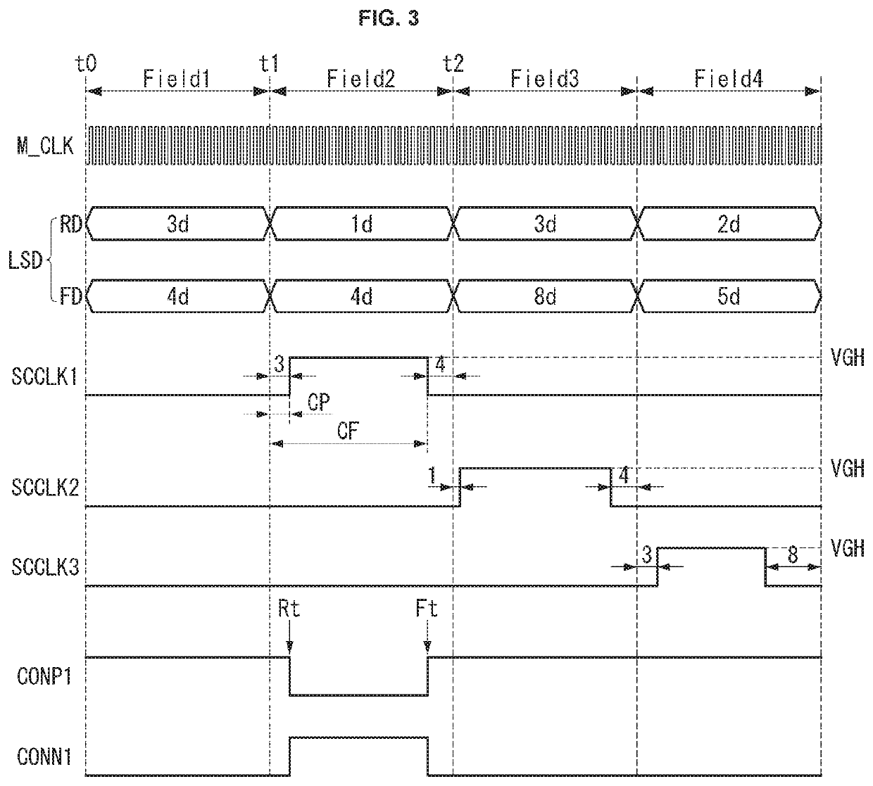
[0047]The counter 411 receives the main clock M_CLK and the control data LSD and counts the main clock M_CLK according to information of the control data LSD belonging to one field to adjust a timing of first and second buffer control signals CONP and CONN.
[0048]Each of the fields Field1 to Field4 may be set to a period for dri...
second embodiment
[0062]As illustrated in FIG. 5, the gate clock generator 400 includes a logic unit LOGIC2, first and second multiplexers MUX1 and MUX2, and a buffer unit BUF2.
[0063]The logic unit LOGIC2 includes a counter 411, a buffer control signal generator 412, and a multiplexer controller 414. The counter 411 and the buffer control signal generator 412 included in the logic unit LOGIC2 may have the same configuration and perform the same operation as those of the first embodiment described above. That is, although not shown inFIG. 6, the logic unit LOGIC2 according to the second embodiment may output the first buffer control signal CONP and the second buffer control signal CONN on the basis of the rising data RD and the falling data FD illustrated in FIG. 3. The multiplexer controller 414 adjusts the number of switches to be turned on included in the first and second multiplexers MUX1 and MUX2 on the basis of slew rate control data SD of the control data LSD. The operation of the multiplexer ...
third embodiment
[0077]The gate clock generator will be described with reference to FIGS. 11 to 13.
[0078]The gate clock generator LS3 according to the third embodiment includes a logic unit LOGIC 3 and a buffer unit BUF 3.
[0079]The logic unit LOGIC 3 includes a counter 411, a buffer control signal generator 412, a GPM control signal generator 415, and a GPM controller 416.
[0080]The counter 411 and the buffer control signal generator 412 of the logic unit LOGIC 3 may have the same configuration and perform the same operation as those of the first embodiment described above. That is, although rising data and falling data are not shown in FIG. 11, the logic unit LOGIC3 according to the third embodiment may output the first buffer control signal CONP and the second buffer control signal CONN on the basis of the rising data RD and the falling data FD illustrated in FIG. 3.
[0081]The GPM control signal generator 415 receives first GPM control data GPMD1 and adjusts a modulation timing of the scan clock SC...
PUM
 Abstract
Description
Claims
Application Information
 - R&D
- Intellectual Property
- Life Sciences
- Materials
- Tech Scout
- Unparalleled Data Quality
- Higher Quality Content
- 60% Fewer Hallucinations
Browse by: Latest US Patents, China's latest patents, Technical Efficacy Thesaurus, Application Domain, Technology Topic, Popular Technical Reports.
© 2025 PatSnap. All rights reserved.Legal|Privacy policy|Modern Slavery Act Transparency Statement|Sitemap|About US| Contact US: help@patsnap.com


