Electronic device and method of manufacturing electronic device, and electronic apparatus

a technology of electronic devices and manufacturing methods, applied in the direction of electroluminescent light sources, organic semiconductor devices, electric lighting sources, etc., can solve the problems of difficult to achieve the intended insulating property of wiring patterns, and achieve the effect of easy and reliable repair and disconnection of short-circuit defects

Active Publication Date: 2020-01-02
SONY CORP
View PDF3 Cites 0 Cited by
  • Summary
  • Abstract
  • Description
  • Claims
  • Application Information

AI Technical Summary

Benefits of technology

[0009]Accordingly, it is desirable to provide an electronic device and a manufacturing method thereof, as well as an electronic apparatus that allow to achieve both of high quality and high manufacturing yield.
[0016]In the electronic device and the manufacturing method thereof, as well as the electronic apparatus of the technology, the plurality of first wiring patterns on which the organic insulating layer and the second wiring pattern are provided in this order in an upper layer thereof are disposed to be electrically coupled to each other partially, and to each extend in the first direction. This makes it possible to perform a short-circuit defect inspection, as well as disconnecting and repair of a detected short-circuit defect at the stage where the first wiring patterns are already formed.
[0017]According to the electronic device and the manufacturing method thereof, as well as the electronic apparatus of the respective embodiments of the technology, in the plurality of first wiring patterns and the second wiring pattern that are laminated with the organic insulating layer interposed between, the plurality of first wiring patterns that are provided in a lower layer of the organic insulating layer are disposed to be electrically coupled to each other partially, and to each extend in the first direction. This makes it possible to inspect the presence or absence of a short-circuit defect in the first wiring patterns, as well as to disconnect and repair a detected short-circuit defect at the stage where the first wiring patterns are already disposed. This makes it possible to provide the electronic device achieving both of the quality and the manufacturing yield, and the electronic apparatus that includes such an electronic device. It is to be noted that effects of the embodiments of the technology are not necessarily limited to the effects described above, and may include any of effects that will be described in the disclosure.

Problems solved by technology

However, in the method mentioned in PTL 2, although superior insulating property has been achieved in disconnecting and repairing a short-circuit part in wiring patterns that are provided on an upper layer of the organic resin layer (on the organic resin layer), it has been difficult to achieve the intended insulating property for wiring patterns that are provided in a lower layer of the organic resin layer.

Method used


Image

  • Electronic device and method of manufacturing electronic device, and electronic apparatus
  • Electronic device and method of manufacturing electronic device, and electronic apparatus
  • Electronic device and method of manufacturing electronic device, and electronic apparatus

Examples


embodiment

1. EMBODIMENT

(1-1. Overall Configuration)

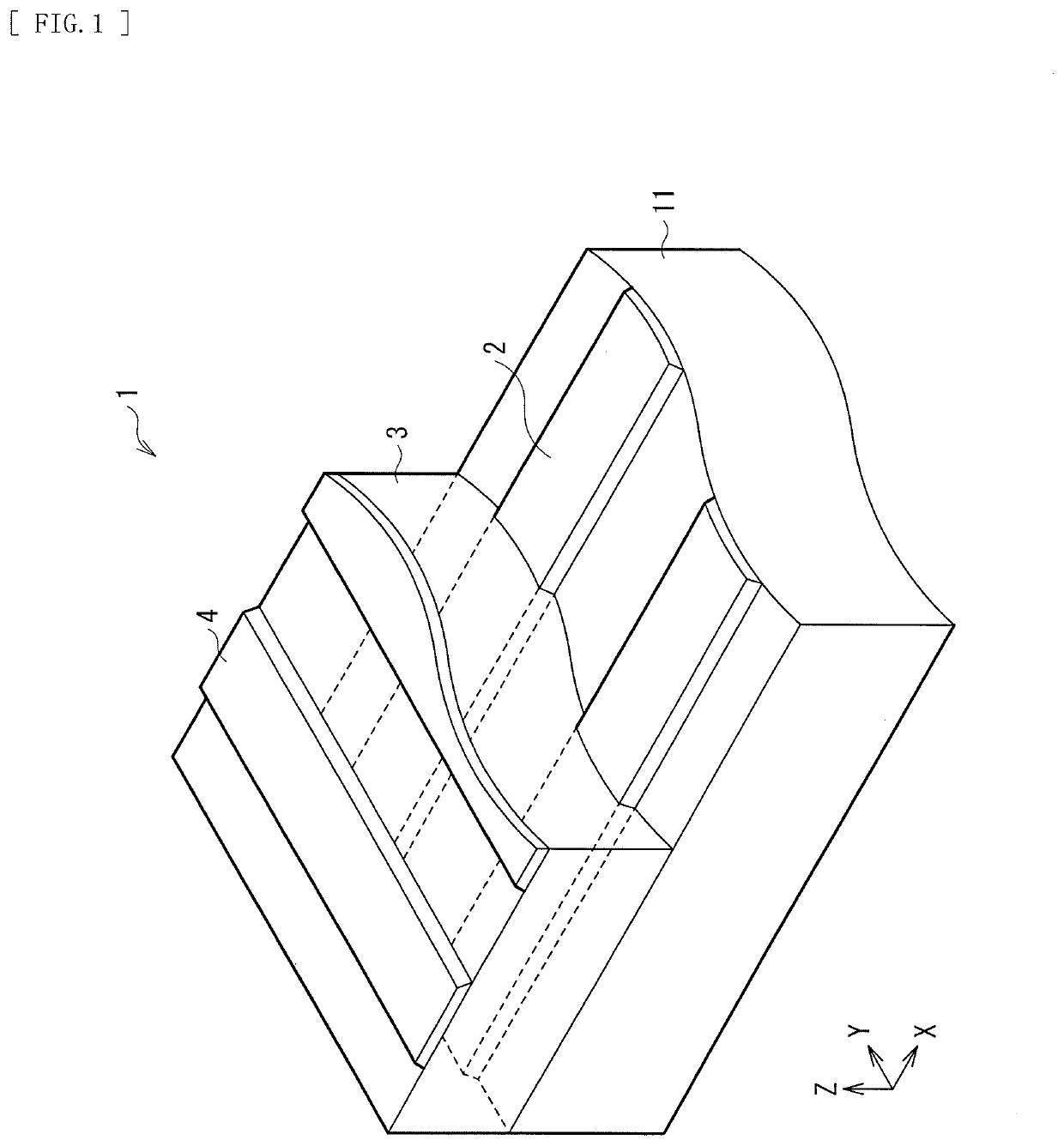
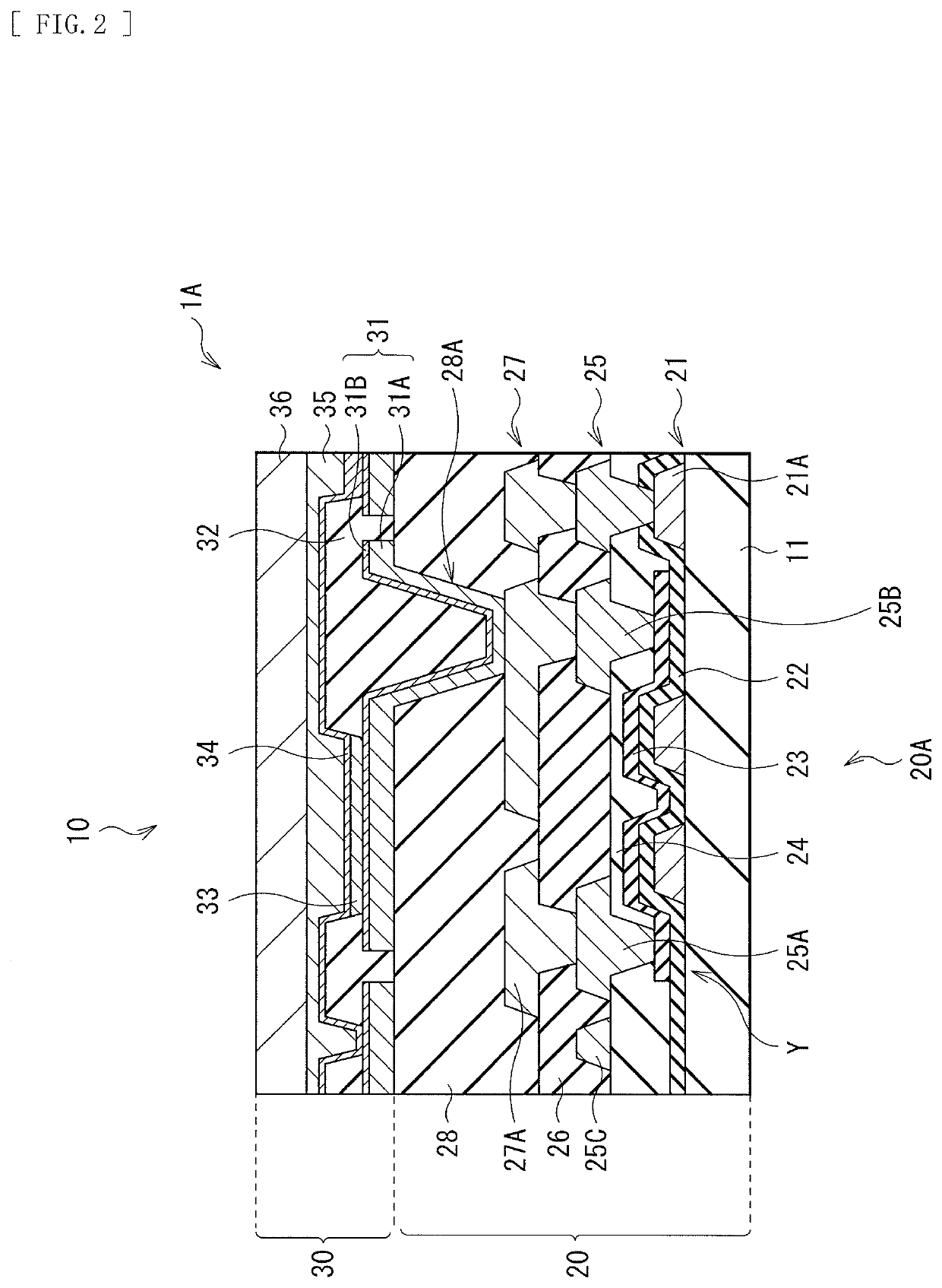
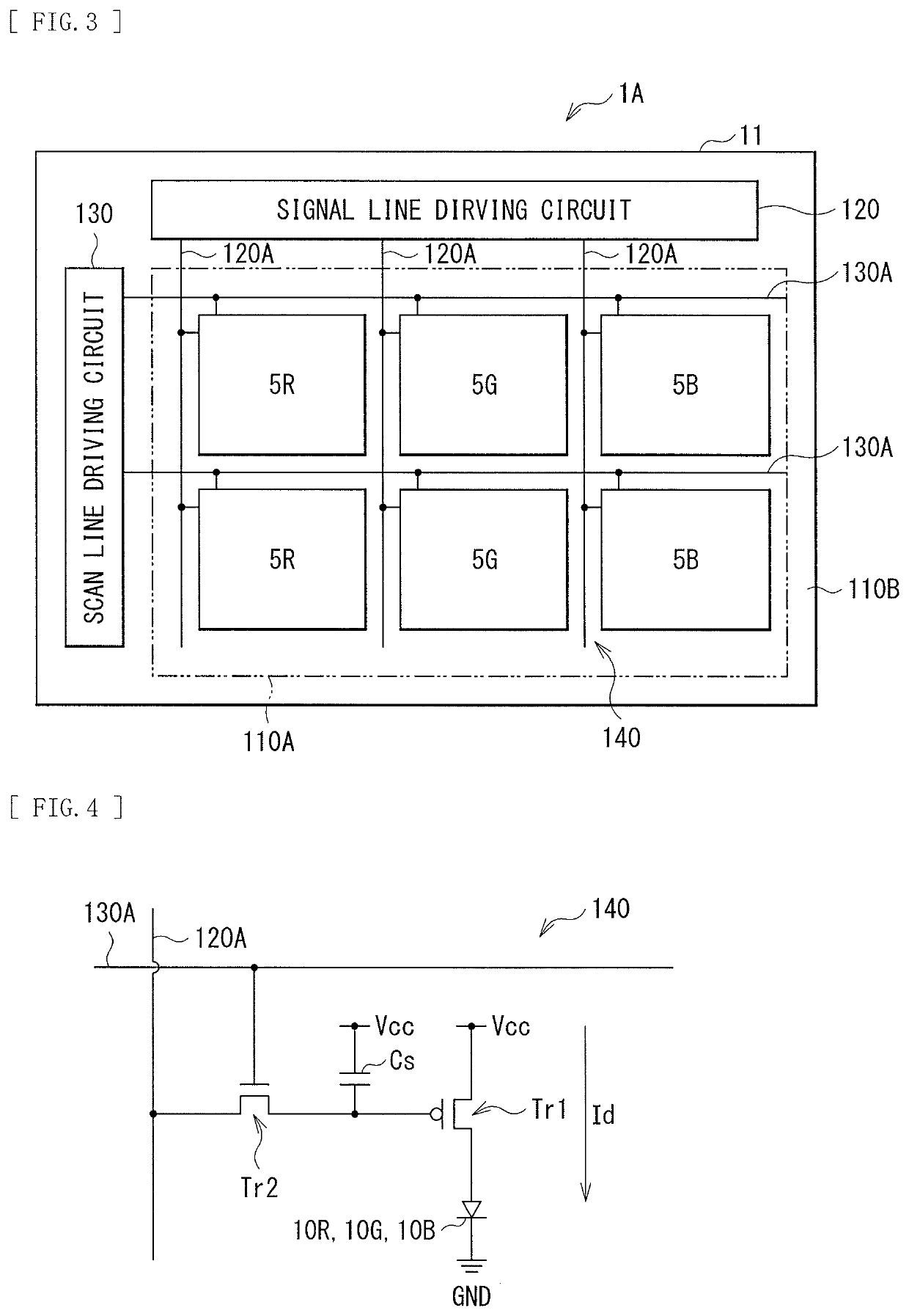
[0037]FIG. 1 illustrates a perspective view of a cross-sectional configuration of an electronic device (an electronic device 1) according to an embodiment of the disclosure. In the electronic device, a lower-layer wiring pattern 2 (a first wiring pattern) and an upper-layer wiring pattern 4 (a second wiring pattern) are laminated with an organic insulating layer 3 interposed between. The plurality of lower-layer wiring patterns 2 are provided on a substrate 11. The lower-layer wiring patterns 2 are disposed in such a manner that the lower-layer wiring patterns 2 are electrically coupled to each other partially, and each extend in one direction, for example, X-axis direction (a first direction). FIG. 2 illustrates a cross-sectional configuration of a display unit (a display unit 1A) that includes a display device that is an example of the electronic device 1 illustrated in FIG. 1. The display unit 1A may be used as, for example, an organic EL ...

application examples

2. APPLICATION EXAMPLES

[0078]The electronic device 1 (for example, the display unit 1A provided with a display device) that is described in the above-described embodiment may be preferably usable optimally as the following electronic apparatuses, for example.

application example 1

[0079]FIG. 10A illustrates an external appearance a tablet to which the display unit 1A according to the above-described embodiment is applied viewed from front side thereof, and FIG. 10B illustrates the external appearance of the tablet viewed from rear side thereof. This tablet may include, for example, a display section 610 (the display unit 1A) and a non-display section (a chassis) 620, as well as an operation section 630. The operation section 630 may be provided on the front surface of the non-display section 620 as illustrated in FIG. 10A, or may be provided on the top surface as illustrated in FIG. 10B.


PUM

PropertyMeasurementUnit
thicknessaaaaaaaaaa
thicknessaaaaaaaaaa
voltageaaaaaaaaaa

Abstract

An electronic device of the technology includes: a plurality of first wiring patterns that are electrically coupled to each other partially, and each extend in a first direction; an organic insulating layer that is provided on the first wiring patterns; and a second wiring pattern that is provided on the organic insulating layer.

Description

CROSS REFERENCE TO RELATED APPLICATIONS[0001]This is a Continuation Application of U.S. patent application Ser. No. 15 / 321,343, filed Dec. 22, 2016, which is a National Stage Entry of Application No.: PCT / JP2015 / 067136, filed Jun. 15, 2015, which claims priority to Japanese Patent Application No.: 2014-146855, filed Jul. 17, 2014, the entire contents of which being incorporated herein by reference.TECHNICAL FIELD[0002]The technology relates to an electronic device having a structure in which a plurality of wiring patterns are laminated with an organic insulating layer interposed between, to a method of manufacturing such an electronic device, and to an electronic apparatus that includes such an electronic device.BACKGROUND ART[0003]In recent years, in an electronic device, the number of wiring patterns has been increased to improve the performance thereof, and circuits have become complex accordingly. In particular, in a display device used for an organic EL (Electroluminescence) di...

Claims


Application Information

Patent Timeline
Patent Type & Authority Applications(United States)
IPC IPC(8): H01L27/32H01L51/00
CPCH01L2251/5392H01L2227/323H01L27/1244H01L27/3262H01L27/3258H01L27/3276H01L51/0031H05B33/22H05B33/26H01L2924/0002H10K59/124H10K59/131H10K71/70H10K50/844H10K2102/341H10K71/861H01L2924/00H10K59/1213H10K59/1201
Inventor NAGASAWA, KOICHIFUJIOKA, HIROFUMIHONDA, TOMOAKI
Owner SONY CORP
Why Eureka
Try Eureka