Waveguide Antenna Element-Based Beam Forming Phased Array Antenna System for Millimeter Wave Communication

Active Publication Date: 2019-08-29
SILICON VALLEY BANK
View PDF0 Cites 12 Cited by
  • Summary
  • Abstract
  • Description
  • Claims
  • Application Information

AI Technical Summary

Benefits of technology

This patent describes a beam forming phased array antenna system for millimeter wave communication. The system uses a waveguide antenna element, which has advantages over other antenna systems. The technical effects of this patent are improved efficiency and accuracy of millimeter wave communication using a beam forming phased array antenna system with a waveguide antenna element.

Problems solved by technology

Although some of the existing antenna arrays exhibit low loss, however, mass production of such antenna arrays that comprise multiple antenna elements may be difficult and pose certain practical and technical challenges.
For example, the multiple antenna elements (usually more than hundred) in an antenna array, needs to be soldered on a substrate during fabrication, which may be difficult and a time-consuming process.
This adversely impacts the total cycle time to produce an antenna array.
Further, assembly and packaging of such large sized antenna arrays may be difficult and cost intensive task.

Method used


Image

  • Waveguide Antenna Element-Based Beam Forming Phased Array Antenna System for Millimeter Wave Communication
  • Waveguide Antenna Element-Based Beam Forming Phased Array Antenna System for Millimeter Wave Communication
  • Waveguide Antenna Element-Based Beam Forming Phased Array Antenna System for Millimeter Wave Communication

Examples


Embodiment Construction

[0031]Certain embodiments of the disclosure may be found in a waveguide antenna element based beam forming phased array antenna system for millimeter wave communication. In the following description, reference is made to the accompanying drawings, which form a part hereof, and in which is shown, by way of illustration, various embodiments of the present disclosure.

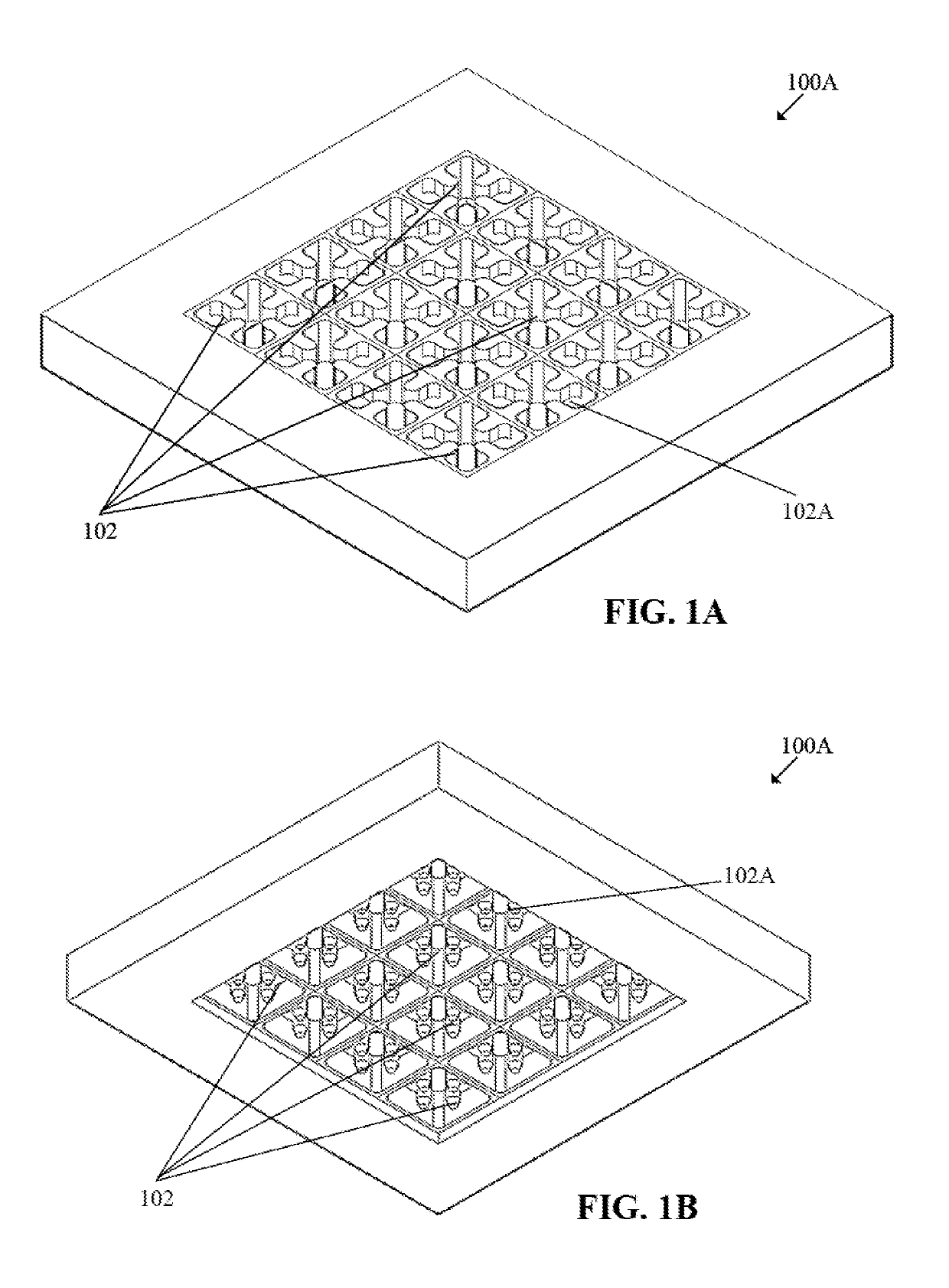
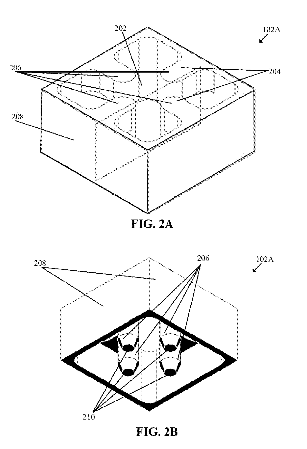
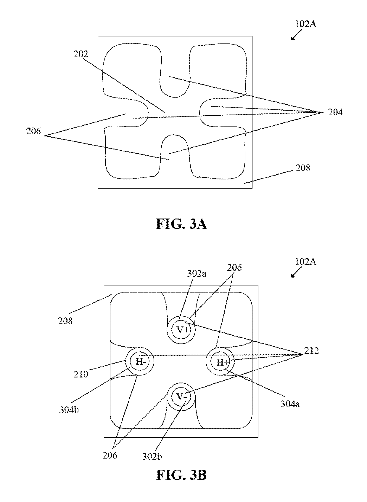
[0032]FIG. 1A depicts a perspective top view of an exemplary waveguide antenna element based beam forming phased array antenna system for millimeter wave communication, in accordance with an exemplary embodiment of the disclosure. With reference to FIG. 1A, there is shown a waveguide antenna element based beam forming phased array 100A. The waveguide antenna element based beam forming phased array 100A may have a unitary body that comprises a plurality of radiating waveguide antenna cells 102 arranged in a certain layout for millimeter wave communication. The unitary body refers to one-piece structure of the waveguide ante...


PUM


Abstract

An antenna system, includes a first substrate, a plurality of chips, and a waveguide antenna element based beam forming phased array. The waveguide antenna element based beam forming phased array has a unitary body that comprises a plurality of radiating waveguide antenna cells in a first layout for millimeter wave communication. Each radiating waveguide antenna cell comprises a plurality of pins that are connected with a body of a corresponding radiating waveguide antenna cell that acts as ground for the plurality of pins. A first end of the plurality of radiating waveguide antenna cells of the waveguide antenna element based beam forming phased array, as the unitary body, in the first layout is mounted on the first substrate. The plurality of chips are electrically connected with the plurality of pins and the ground of each of the plurality of radiating waveguide antenna cells to control beamforming.

Description

CROSS-REFERENCE TO RELATED APPLICATIONS / INCORPORATION BY REFERENCE[0001]This Patent Application makes reference to, claims priority to, claims the benefit of, and is a Continuation Application of U.S. patent application Ser. No. 15 / 904,521, filed Feb. 26, 2018.[0002]This Application makes reference to:[0003]U.S. application Ser. No. 15 / 607,743, which was filed on May 30, 2017; and[0004]U.S. application Ser. No. 15 / 834,894, which was filed on Dec. 7, 2017.[0005]Each of the above referenced Application is hereby incorporated herein by reference in its entirety.FIELD OF TECHNOLOGY[0006]Certain embodiments of the disclosure relate to an antenna system for millimeter wave-based wireless communication. More specifically, certain embodiments of the disclosure relate to a waveguide antenna element based beam forming phased array antenna system for millimeter wave communication.BACKGROUND[0007]Wireless telecommunication in modern times has witnessed advent of various signal transmission tech...

Claims


Application Information

Patent Timeline
IPC IPC(8): H01Q21/22H01Q21/00H01Q1/02H01Q3/34H01Q1/52H01Q13/20
CPCH01Q21/22H01Q21/0025H01Q13/20H01Q3/34H01Q1/523H01Q1/02H01Q21/24H01Q21/064
Inventor YOON, SEUNGHWANROFOUGARAN, AHMADREZAGHARAVI, SAMSRIDHARAN, KARTIKSHIN, DONGHYUPSHIRINFAR, FARIDWU, STEPHENROFOUGARAN, MARYAMBESOLI, ALFRED GRAUADAS, ENVERWANG, ZHIHUI
Owner SILICON VALLEY BANK
Why Eureka
Try Eureka