
Light-emitting diode package

a technology of light-emitting diodes and package parts, which is applied in the direction of basic electric elements, electrical apparatus, and semiconductor devices, can solve the problems of serious color halo phenomenon in the vehicle headlights, other side effects, and other problems, and achieve the effect of improving luminous efficacy and weather resistance, and controlling the width of the concave grooves

Active Publication Date: 2019-08-08
LEXTAR ELECTRONICS CORP
View PDF1 Cites 0 Cited by
  • Summary
  • Abstract
  • Description
  • Claims
  • Application Information

AI Technical Summary

Benefits of technology

The present invention is a new type of LED package that uses a cavity to prevent damage caused by differences in expansion and contraction between the layers. This cavity acts as a buffer space and allows the layers to expand and contract without causing damage. By controlling the width of the cavity, the LED package can improve its efficiency and resistance to weather.

Problems solved by technology

Although the ceramic phosphor sheet may solve the thermal cracking problem, other side effects are also accompanied.
When a difference between CTEs (Coefficient of thermal expansion) of the ceramic phosphor sheet and the light-reflective material is too large, in the state of long-time lighting or excessive temperature difference, the light-reflective material may expand to press and damage the ceramic phosphor sheet, and the ceramic phosphor sheet is thus cracked to have its fluorescent powders peeled off, thereby causing a serious color halo phenomenon in the vehicle headlight.

Method used


Image

  • Light-emitting diode package
  • Light-emitting diode package
  • Light-emitting diode package

Examples


Embodiment Construction

[0022]Reference will now be made in detail to the present embodiments of the invention, examples of which are illustrated in the accompanying drawings. Wherever possible, the same reference numbers are used in the drawings and the description to refer to the same or like parts.

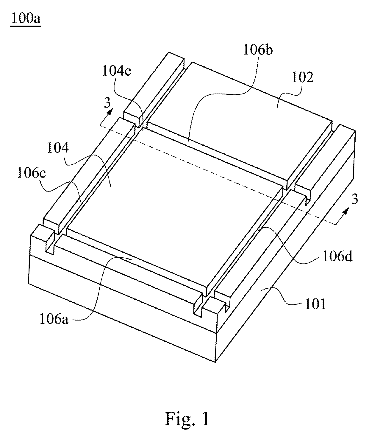
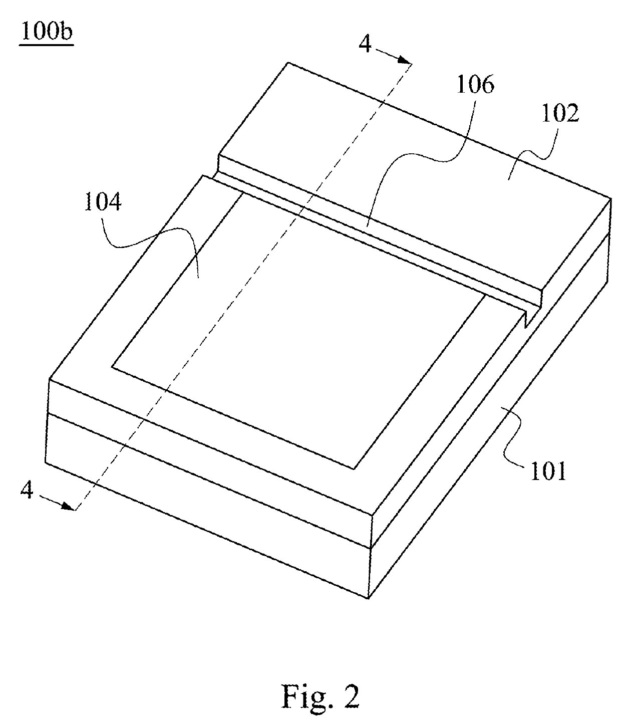
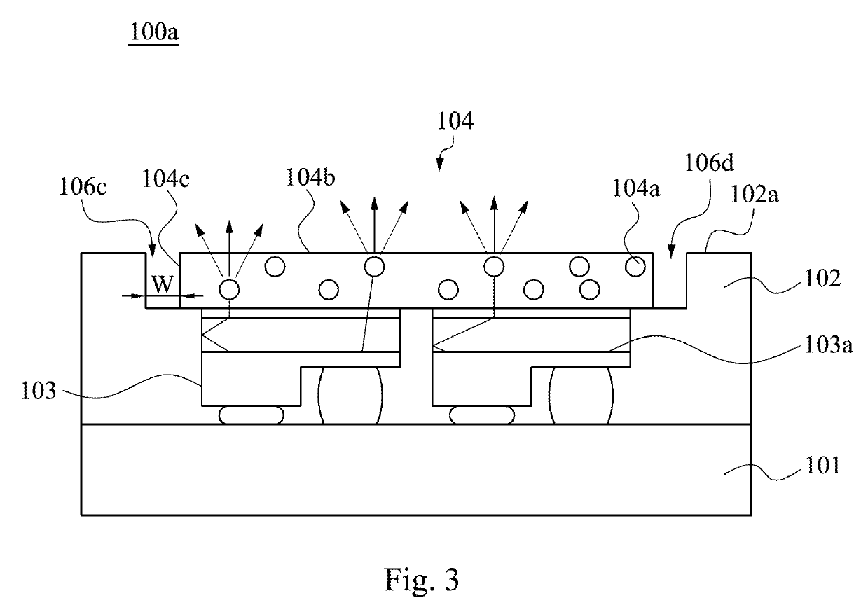
[0023]Reference is made to FIG. 1, which illustrates a perspective view of a light-emitting diode package according to one embodiment of the present disclosure. A light-emitting diode package 100a includes a substrate 101, at least one light-emitting chip 103 (referring to FIG. 3), a light-reflective layer 102 and a wave-length conversion fluorescent layer 104. The light-reflective layer 102 surrounds the light-emitting chip 103 and all edges of the wave-length conversion fluorescent layer 104. The wave-length conversion fluorescent layer 104 is located over the light-emitting chip 103, and configured to convert light emitted from the light-emitting chip 103 into light with different colors or wave-lengths. An...


PUM


Abstract

A light-emitting diode package includes a substrate, at least one light-emitting chip, a light-reflective layer and a wave-length conversion fluorescent layer. The light-emitting chip is located on the substrate. The light-reflective layer is arranged around the light-emitting chip. The wave-length conversion fluorescent layer is located over the light-emitting chip, wherein the light-reflective layer is spaced from the fluorescent wave-length conversion layer by a groove that reaches two opposite sides of the light-emitting diode package.

Description

CROSS-REFERENCE TO RELATED APPLICATION[0001]This application claims priority to China Application Serial Number 201810128340.0, filed Feb. 8, 2018 which is herein incorporated by reference in its entirety.BACKGROUNDField of Invention[0002]The present disclosure relates to a light-emitting diode package.Description of Related Art[0003]Some conventional light-emitting diode vehicle headlights may have a high luminous intensity per unit area, and the inorganic sintering technology is often used on the photoelectric conversion material, and the phosphor powders are made into a ceramic composite sheet in order to solve the thermal cracking problem of the silicone based fluorescent layer.[0004]Although the ceramic phosphor sheet may solve the thermal cracking problem, other side effects are also accompanied. When a difference between CTEs (Coefficient of thermal expansion) of the ceramic phosphor sheet and the light-reflective material is too large, in the state of long-time lighting or e...

Claims


Application Information

Patent Timeline
Patent Type & Authority Applications(United States)
IPC IPC(8): H01L33/50H01L33/60H01L33/62H01L25/075
CPCH01L33/505H01L33/60H01L33/62H01L25/0753H01L33/48H01L33/56H01L2933/0041
Inventor TSAI, SHANG-HSUNLIU, LI-WEI
Owner LEXTAR ELECTRONICS CORP
Learn More