Electroluminescence display device

Active Publication Date: 2019-07-04
LG DISPLAY CO LTD
View PDF6 Cites 13 Cited by
  • Summary
  • Abstract
  • Description
  • Claims
  • Application Information

AI Technical Summary

Benefits of technology

The present invention aims to provide an electroluminescent display device that can save time by reducing the number of spraying times of a solution for forming an emission layer through an inkjet apparatus. Additionally, it aims to overcome the issue of dark spots in a specific pixel by creating a uniform profile of the emission layer.

Problems solved by technology

Accordingly, in order to realize the large thickness of the red (R) emitting layer 51 by the solution process, a solution has to be sprayed several times through a nozzle of the inkjet apparatus, thereby causing an increase of process time.
Also, if the blue (B) emitting layer 53 has the small thickness resulting from the solution process, it is difficult to realize uniformity of profile of the blue (B) emitting layer 53, which might cause a possibility of a dark spot in a blue pixel.

Method used


Image

  • Electroluminescence display device
  • Electroluminescence display device
  • Electroluminescence display device

Examples


Embodiment Construction

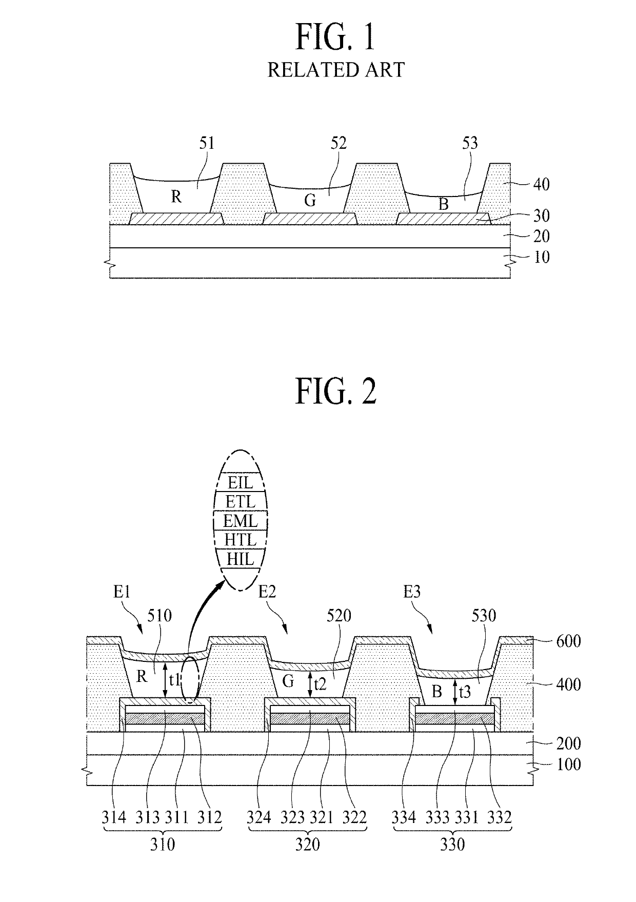
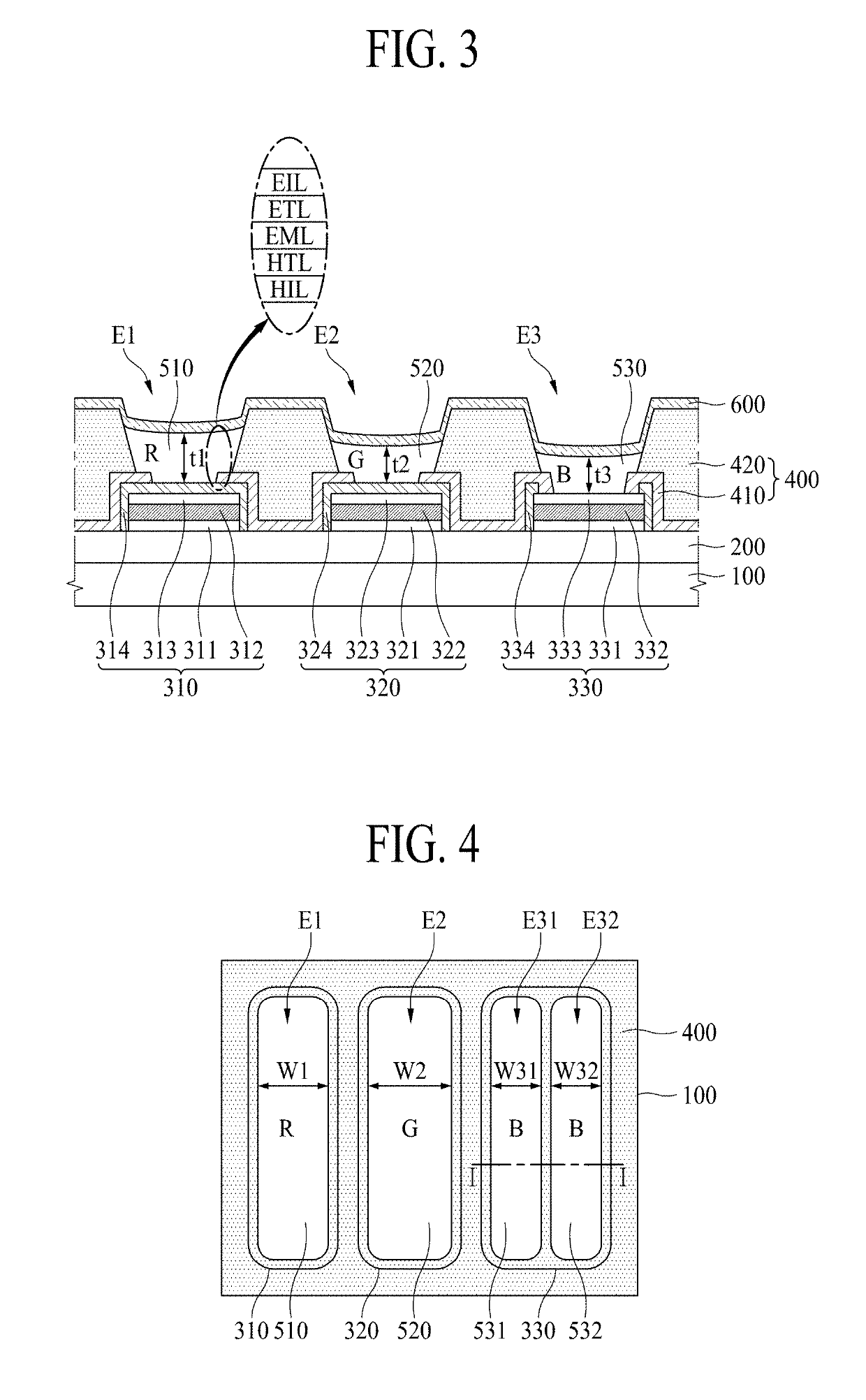
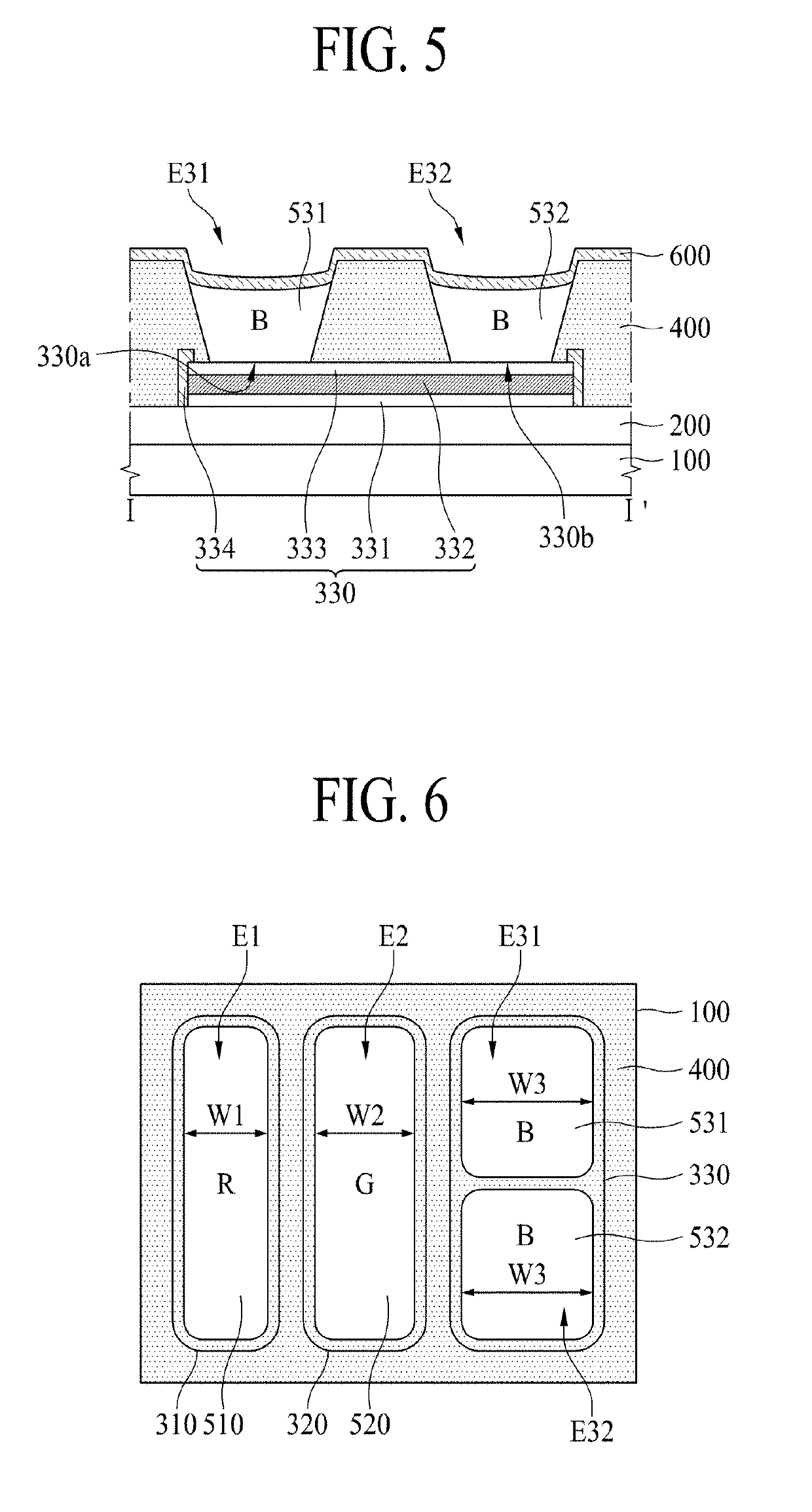
[0035]Advantages and features of the present disclosure, and implementation methods thereof will be clarified through the following aspects, described with reference to the accompanying drawings. The present disclosure may, however, be embodied in different forms and should not be construed as being limited to the aspects set forth herein. Rather, these aspects are provided so that this disclosure will be thorough and complete, and will fully convey the scope of the present disclosure to those skilled in the art. Further, the present disclosure is only defined by the scope of the claims.

[0036]The shapes, sizes, ratios, angles, and numbers disclosed in the drawings for describing aspects of the present disclosure are merely examples, and thus the present disclosure is not limited to the illustrated details. Like reference numerals refer to like elements throughout. In the following description, when the detailed description of the relevant known function or configuration is determine...


PUM


Abstract

An electroluminescent display device includes a substrate, a bank provided on the substrate and configured to define a first emission area and a second emission area, a first emission layer provided in the first emission area, a second emission layer provided in the second emission area, a first electrode provided below the first emission layer, and a second electrode provided below the second emission layer, wherein a thickness of a first portion of the first electrode is larger than a thickness of a first portion of the second electrode.

Description

CROSS REFERENCE TO RELATED APPLICATION[0001]This application claims the benefit under 35 U.S.C. § 119(a) of Korean Patent Application No. 10-2017-0184316 filed on Dec. 29, 2017, which is incorporated herein by reference in its entirety.BACKGROUNDField of the Disclosure[0002]The present disclosure relates to an electroluminescent display device, and more particularly, to an electroluminescent display device having an emission layer manufactured by a solution process.Description of the Background[0003]An electroluminescent display device is provided in such way that an emission layer is formed between two electrodes. As the emission layer emits light due to an electric field between the two electrodes, an image is displayed on the electroluminescent display device.[0004]The emission layer may be formed of an organic material which emits light when an exciton is produced by a bond of an electron and a hole, and the exciton falls to a ground state from an excited state, or may be formed...

Claims


Application Information

Patent Timeline
IPC IPC(8): H01L51/52H01L27/32H01L51/00H01L51/50
CPCH01L51/5265H01L27/3223H01L27/3246H01L27/3262H01L27/3272H01L27/3276H01L51/0005H01L51/5012H01L51/5209H01L51/5218H01L51/5088H01L51/5056H01L27/1225H01L29/7869H01L29/78633H01L2251/308H01L2251/5315H01L2251/558H10K59/12H10K50/805G09G2300/0452G09G2300/0426G09G3/32G09G2300/0842G09G2300/0866H10K71/135H10K59/805H10K59/80515H10K59/80521H10K59/876H10K50/11H10K2102/351H10K59/122H10K50/13H10K50/14H10K50/17H10K50/84H10K50/852H10K50/15H10K50/813H10K50/818H10K59/88H10K59/126H10K59/131H10K59/1213H10K2102/103H10K2102/3026
Inventor PAEK, SEUNGHANKIM, SUPHILYEO, JONGHOONLEE, JIHOON
Owner LG DISPLAY CO LTD
Why Eureka
Try Eureka