Light-receiving device, method of manufacturing light-receiving device, imaging device, and electronic apparatus
a technology of light-emitting devices and light-emitting devices, which is applied in the direction of electrical equipment, semiconductor devices, radio frequency controlled devices, etc., to achieve the effects of suppressing the occurrence of color mixture, preventing the movement of signal charges (holes) and preventing the movement of holes over the pixels p
- Summary
- Abstract
- Description
- Claims
- Application Information
AI Technical Summary
Benefits of technology
Problems solved by technology
Method used
Image

Examples
embodiment
Configuration of Light-Receiving Device 10
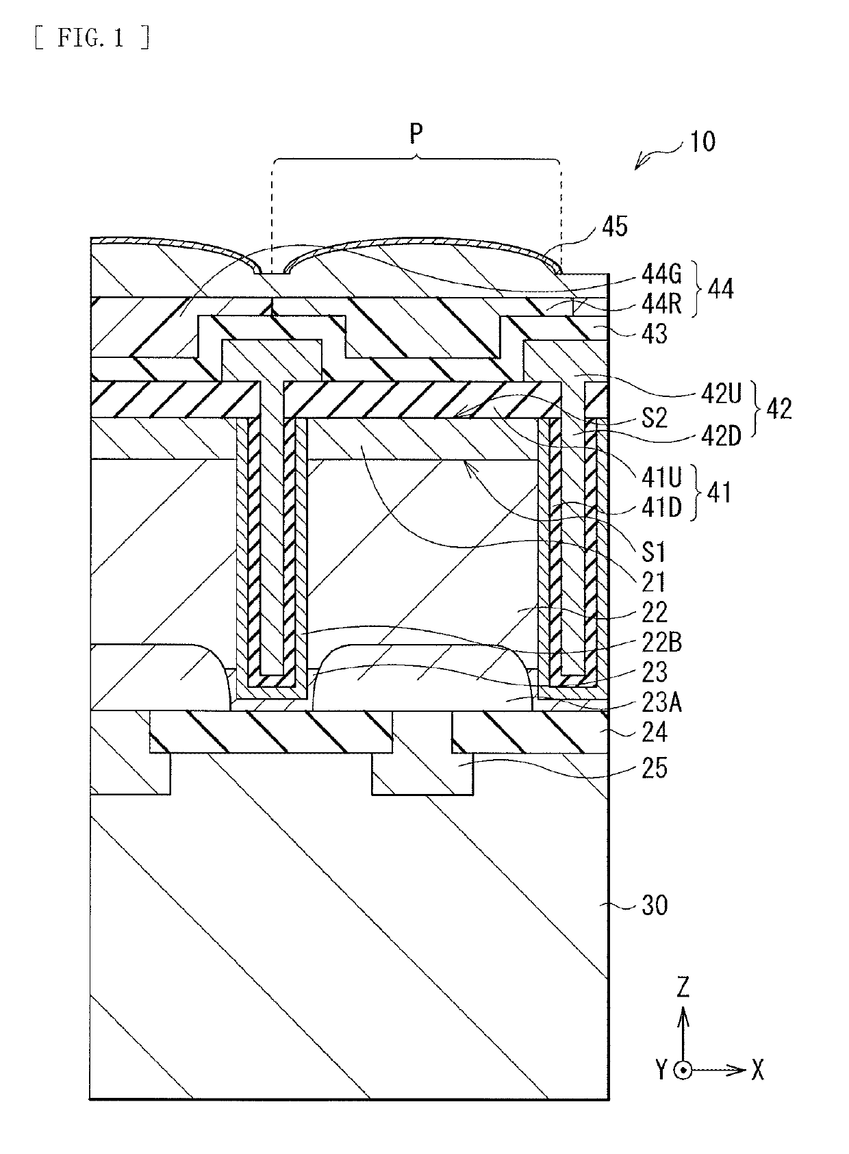
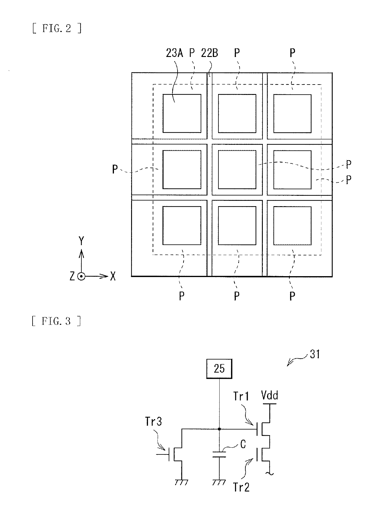
[0042]FIG. 1 illustrates a cross-sectional configuration of a light-receiving device (a light-receiving device 10) according to an embodiment of the present technology. The light-receiving device 10 is applied to, for example, an infrared sensor, etc., and includes a plurality of light-receiving unit regions (serving as pixels P) that are two-dimensionally arranged.
[0043]The light-receiving device 10 includes a substrate 21, and a photoelectric conversion layer 22, a cap layer 23, a first protective layer 24, and a multilayer wiring substrate 30 are provided in this order on one surface (a surface S1) of the substrate 21. A first electrically-conductive type region 23A is provided for each of pixels P in the photoelectric conversion layer 22 and the cap layer 23. The light-receiving device 10 includes an electrode 25 penetrating through the first protective layer 24, and the first electrically-conductive type region 23A and a ROIC (Readout I...
modification example 1
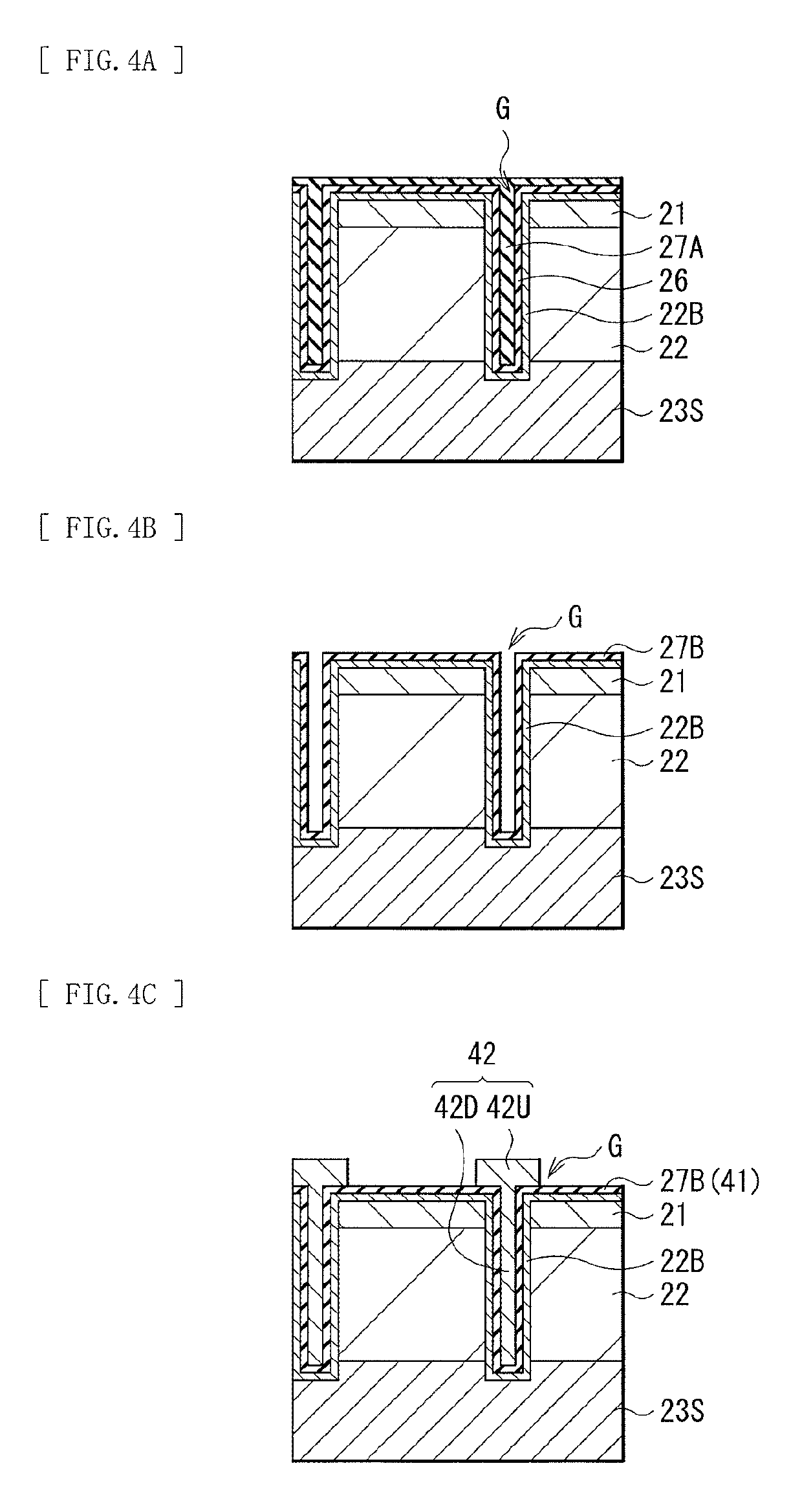
[0091]FIG. 9 illustrates a cross-sectional configuration of a light-receiving device (a light-receiving device 10A) according to a modification example 1. In the light-receiving device 10A, the insulating film (the insulating film 41D in FIG. 1) is not provided in the photoelectric conversion layer 22. Except for this point, the light-receiving device 10A has a configuration similar to that of the light-receiving device 10, and workings and effects are also similar.
[0092]As with the light-receiving device 10, the light-receiving device 11A includes the light-blocking structure 42D in the photoelectric conversion layer 22, and the second electrically-conductive type region 22B is provided around the light-blocking structure 42D. In other words, a separation structure between the pixels P includes the second electrically-conductive type region 22B and the light-blocking structure 42D. As with the light-receiving device 10, such a light-receiving device 10A also prevents movement of si...
modification example 2
[0093]FIG. 10 illustrates a cross-sectional configuration of a light-receiving device (a light-receiving device 10B) according to a modification example 2. In the light-receiving device 10B, the light-blocking structure (the light-blocking structure 42D in FIG. 1) is not provided in the photoelectric conversion layer 22. Except for this point, the light-receiving device 10B has a configuration similar to that of the light-receiving device 10, and workings and effects thereof are also similar.
[0094]As with the light-receiving device 10, the light-receiving device 10B includes the insulating film 41D in the photoelectric conversion layer 22, and the second electrically-conductive type region 22B is provided around the insulating film 41D. In other words, a separation structure between the pixels P includes the second electrically-conductive type region 22B and the insulating film 41D. As with the light-receiving device 10, such a light-receiving device 10B also prevents movement of si...
PUM
 Abstract
Description
Claims
Application Information
 - R&D
- Intellectual Property
- Life Sciences
- Materials
- Tech Scout
- Unparalleled Data Quality
- Higher Quality Content
- 60% Fewer Hallucinations
Browse by: Latest US Patents, China's latest patents, Technical Efficacy Thesaurus, Application Domain, Technology Topic, Popular Technical Reports.
© 2025 PatSnap. All rights reserved.Legal|Privacy policy|Modern Slavery Act Transparency Statement|Sitemap|About US| Contact US: help@patsnap.com