
Electronic element with embedded information

a technology of embedded information and electronic elements, applied in the direction of dielectric characteristics, semiconductor/solid-state device details, fixed capacitor details, etc., can solve the problems of counterfeiters reverse-engineering the design, the actual materials used to build the integrated circuit processor or thin film device typically cost only a few dollars, and the function performed is difficult to reprodu

Active Publication Date: 2019-06-13
EASTMAN KODAK CO
View PDF5 Cites 9 Cited by
  • Summary
  • Abstract
  • Description
  • Claims
  • Application Information

AI Technical Summary

Benefits of technology

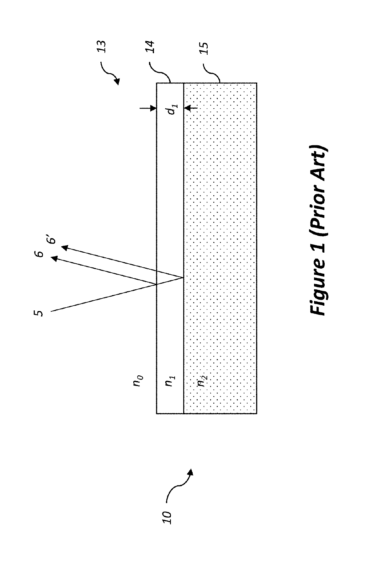
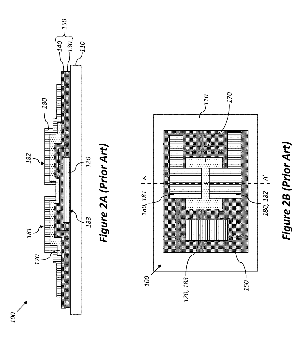
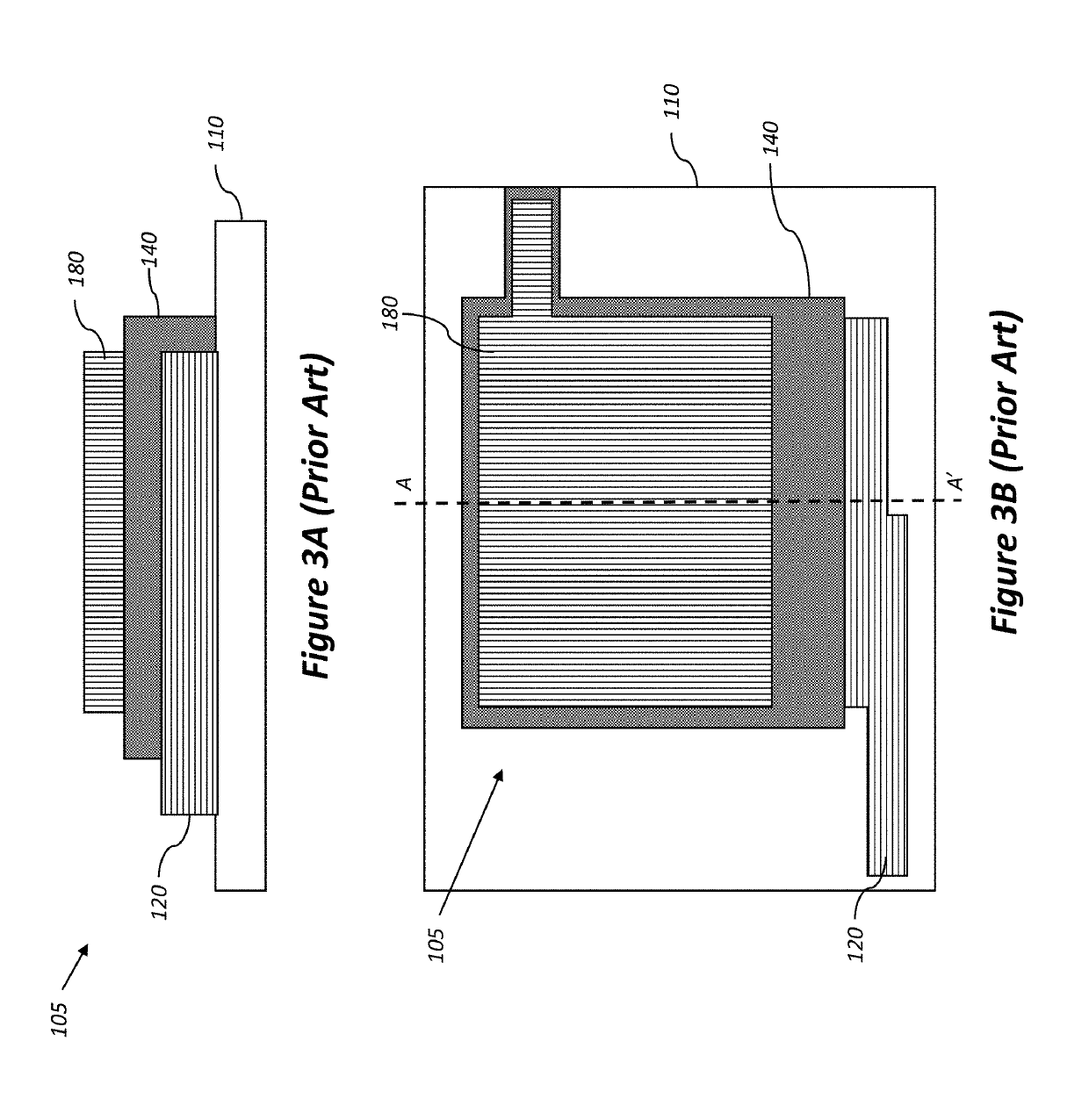
This invention allows for the simultaneous fabrication of an optical layer structure and an electrical element without needing any extra steps. Additionally, the optically-detectable interference image can serve as a way to verify the authenticity of the image, making it difficult to reproduce.

Problems solved by technology

For example, an integrated circuit processor or thin film device often results from an intense and expensive development process, but the actual materials used to build the integrated circuit processor or thin film device typically cost only a few dollars.
In some instances, however, counterfeiters reverse-engineer the design, or the functions performed by the design, to create counterfeit devices.
The presence of counterfeit electronic devices or electronic components within an electronic device presents a number of business risks and security risks.
Manufacturers who have their products counterfeited risk a loss in reputation because of failures associated with counterfeit components.
Components that do not function up to the original manufacture specifications expose the end user to unplanned outages and denial of warranty service, while the manufacturer is exposed to potential liability for fixing systems that the manufacturer did not build or sell.
While a good process for adding indicia, any process that involves a separate printing step to form the decorative image, is easily defeated by the counterfeiter who merely needs to copy the indicia and print the information directly onto the counterfeit electronic devices or electronic device components.
To-date there have been no solutions that have enabled embedded information to be co-located with electrical devices which make use of the properties of the transparent thin-films of today's electronics.

Method used


Image

  • Electronic element with embedded information
  • Electronic element with embedded information
  • Electronic element with embedded information

Examples


Embodiment Construction

[0037]Throughout the specification and claims, the following terms take the meanings explicitly associated herein, unless the context clearly dictates otherwise. The meaning of “a,”“an,” and “the” includes plural reference, the meaning of “in” includes “in” and “on.” Additionally, directional terms such as “on,”“over,”“top,”“bottom,”“left,”“right” are used with reference to the orientation of the figure(s) being described. Because components of embodiments of the present invention can be positioned in a number of different orientations, the directional terminology is used for purposes of illustration only and is in no way limiting.

[0038]The present description will be directed in particular to elements forming part of, or cooperating more directly with, an apparatus in accordance with the present invention. It is to be understood that elements not specifically shown, labeled, or described can take various forms well known to those skilled in the art. In the following description and...


PUM


Abstract

An electrical element includes an optically-detectable pattern of embedded information. A plurality of thin-film layers is applied on the surface of the substrate wherein one or more of the thin-film layers is at least partially transparent. The plurality of thin-film layers overlaps in an encoding region to form an optical layer structure, wherein at least one of the thin-film layers in the optical layer structure contributes to an electrical function of the electrical element. At least one of the thin-film layers in the optical layer structure includes an information-encoding pattern which contributes to an optically-detectable interference image when illuminated by incident light, and wherein the optically-detectable interference image corresponds to at least a portion of the pattern of embedded information.

Description

CROSS-REFERENCE TO RELATED APPLICATIONS[0001]Reference is made to commonly assigned, U.S. patent application Ser. No. ______ (Docket K002207), entitled: “Embedding information in an electronic element,” by C. Ellinger et al.; and to commonly assigned, U.S. patent application Ser. No. ______ (Docket K002208), entitled: “Decoding information embedded in an electronic element,” by C. Ellinger et al., each which is incorporated herein by reference.FIELD OF THE INVENTION[0002]This invention relates generally to thin film electronic devices, and more particularly to thin film electronic devices including embedded optically-detectable information.BACKGROUND OF THE INVENTION[0003]The electronic and manufacturing issues associated with thin film transistors (TFTs) can be viewed as representative of the electronic and manufacturing issues associated with many thin film electrical components. TFTs are widely used as switching elements in electronics, for example, in active-matrix liquid-crysta...

Claims


Application Information

Patent Timeline
Patent Type & Authority Applications(United States)
IPC IPC(8): H05K1/02H01L23/544H01G4/002H01C1/04
CPCH05K1/0269H01L23/544H01G4/002H01C1/04H01L2223/5442H01L2223/54433H01G4/33H05K2201/09936H01C7/006H05K2201/2054H05K1/0274H05K2201/0108
Inventor ELLINGER, CAROLYN RAEFOWLKES, WILLIAM YURICHSPAULDING, KEVIN EDWARD
Owner EASTMAN KODAK CO
Learn More