
Balun circuit arrangement

a circuit arrangement and circuit technology, applied in the direction of waveguide devices, electrical devices, impedence networks, etc., can solve the problems of increased power consumption and/or silicon area, unwanted effects, and inability to control the voltage of the circuit, so as to reduce the effect of injection pulling and avoid the effect of affecting the cost and overall performance of the rf communication application

Active Publication Date: 2019-05-23
QORVO INT PTE LTD
View PDF0 Cites 0 Cited by
  • Summary
  • Abstract
  • Description
  • Claims
  • Application Information

AI Technical Summary

Benefits of technology

The present invention provides an effective solution to mitigate the effects of injection pulling without negative effects on cost and overall performance of the RF communication application. The invention includes a balun circuit arrangement and an oscillator circuit combination that effectively suppresses injection pulling. The balun circuit arrangement includes a series connection of inductive and capacitive impedance elements to provide filtering and balun functions. The first inductive impedance element is directly connected to the negative terminal of the balanced terminals to further lessen the effects of injection pulling. The first and second inductive impedance elements have a higher impedance value in a frequency region around a second harmonic frequency of the oscillator circuit, which also suppresses injection pulling. The combination is especially effective in an embodiment where the oscillator circuit has a direct up-conversion transmitter architecture with a local oscillator operating at twice the output frequency.

Problems solved by technology

This type of transmitter architecture is susceptible to oscillator injection pulling (or oscillator re-modulation), which is an unwanted effect in RF design.
A possible solution to mitigate the effects of injection pulling would be to shift operation of the local oscillator to four times or two thirds of the output frequency, but this will result in increased power consumption and / or increased silicon area (if operating at two thirds of the output frequency).

Method used


Image

  • Balun circuit arrangement
  • Balun circuit arrangement

Examples


Embodiment Construction

[0015]Radiofrequency (RF) communication applications are widespread, and the present invention embodiments relate to specific applications in low energy and moderate to low data rate RF communication applications, such as ZigBee and Bluetooth applications.

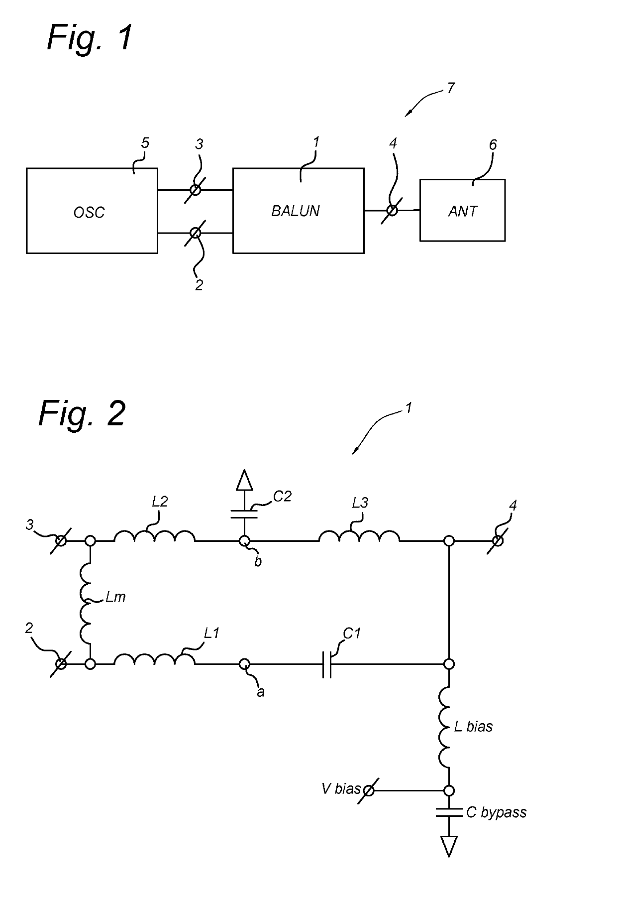
[0016]FIG. 1 shows a block diagram of a common set-up of an RF communication arrangement 7 wherein the present invention embodiments can be applied. Shown are an oscillator circuit 5 providing a balanced output signal as well as an antenna 6 for transmitting (and receiving) RF signals. The oscillator circuit 5 is e.g. implemented as a radio chip, such as a ZigBee or Bluetooth radio chip. In many applications, the antenna 6 is a single ended antenna, and a balun circuit arrangement 1 is used to transform the balanced (or differential) signal from the oscillator circuit 5 to an unbalanced signal to the antenna 6 (and vice versa). In FIG. 1 also the connecting terminals of the balun circuit arrangement 1 are shown, i.e. a balanced por...


PUM


Abstract

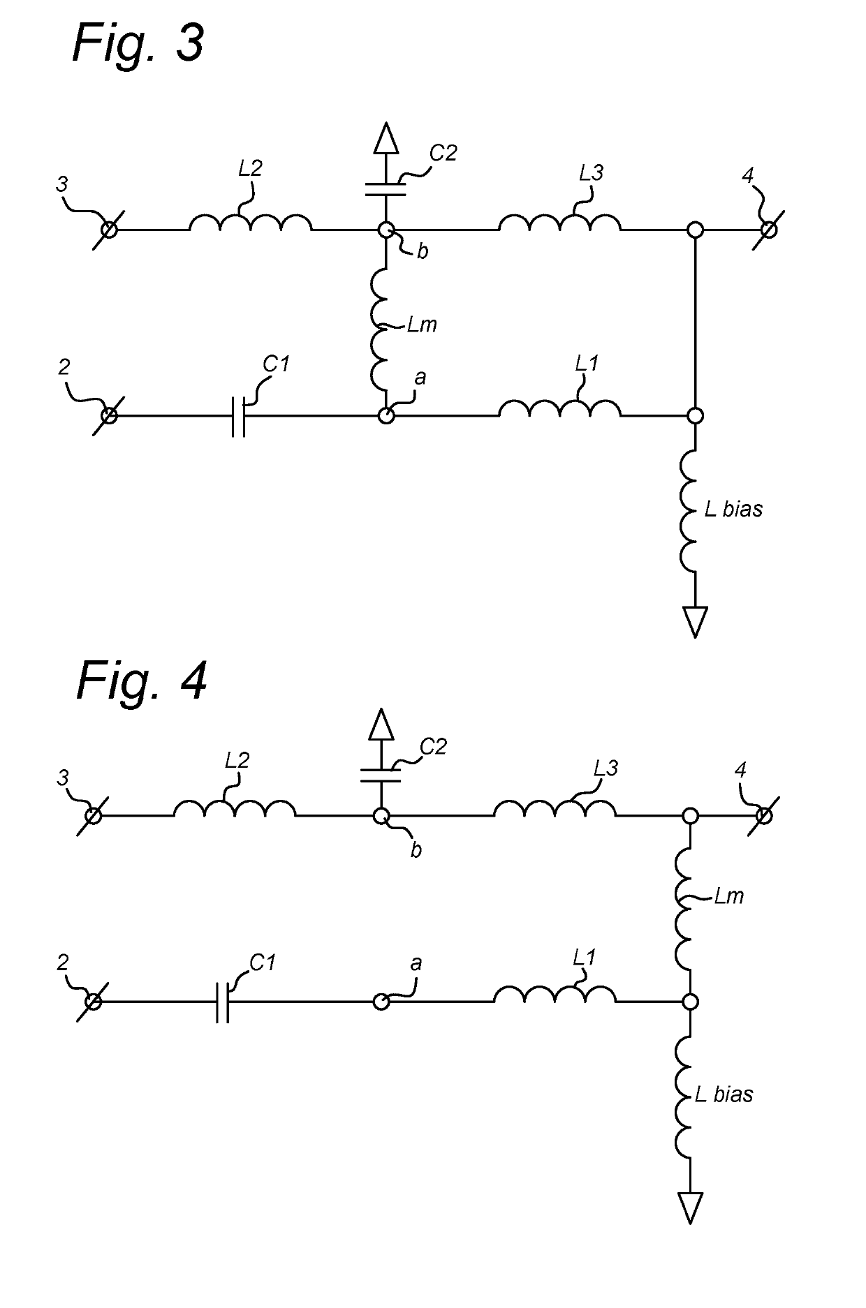
Balun circuit arrangement with a balanced port side having two balanced terminals and an unbalanced port side having an unbalanced terminal. A first series connection of a first inductive impedance element (L1) and a first capacitive impedance element (C1) is present between a negative terminal of the two balanced terminals and the unbalanced terminal. A second series connection of a second inductive impedance element (L2) and a third inductive impedance element (L3) is present between a positive terminal of the two balanced terminals and the unbalanced terminal, and a second capacitive element (C2) is connected between a node connecting the second and third inductive element and a ground connection. The balun circuit arrangement may be used in a combination with an oscillator circuit and a single ended antenna.

Description

TECHNICAL FIELD[0001]The present invention relates to a balun circuit arrangement comprising a balanced port side having two balanced terminals and an unbalanced port side having an unbalanced terminal. In a further aspect, the present invention relates to a combination of an oscillator circuit and a balun circuit arrangement according to any one of the present invention embodiments, wherein the oscillator circuit provides an output signal at an output frequency and is connected to the balanced port side of the balun circuit arrangement.BACKGROUND ART[0002]In many RF communication applications, such as applications according to the ZigBee standard, use is made of a direct up-conversion transmitter architecture wherein a local oscillator is operating at twice the output frequency (operational transmitting frequency). This type of transmitter architecture is susceptible to oscillator injection pulling (or oscillator re-modulation), which is an unwanted effect in RF design. The article...

Claims


Application Information

Patent Timeline
IPC IPC(8): H01P5/10H03H7/42H04B1/04
CPCH01P5/10H03H7/42H04B1/0475
Inventor SHEN, YILONG
Owner QORVO INT PTE LTD
Learn More