Method and electronic device for dynamically changing ground points of a plurality of antennas of the electronic device

a technology of electronic devices and ground points, which is applied in the direction of antenna earthings, independent non-interfering antenna combinations, and particular array feeding systems, etc., can solve the problems of reducing the rate at which the top antenna and the bottom antenna are shifted, and it is nearly impossible or difficult for the electronic device to communicate with any other electronic device, so as to reduce the influence of parasitic curren

Active Publication Date: 2019-02-14
SAMSUNG ELECTRONICS CO LTD
View PDF11 Cites 4 Cited by
  • Summary
  • Abstract
  • Description
  • Claims
  • Application Information

AI Technical Summary

Benefits of technology

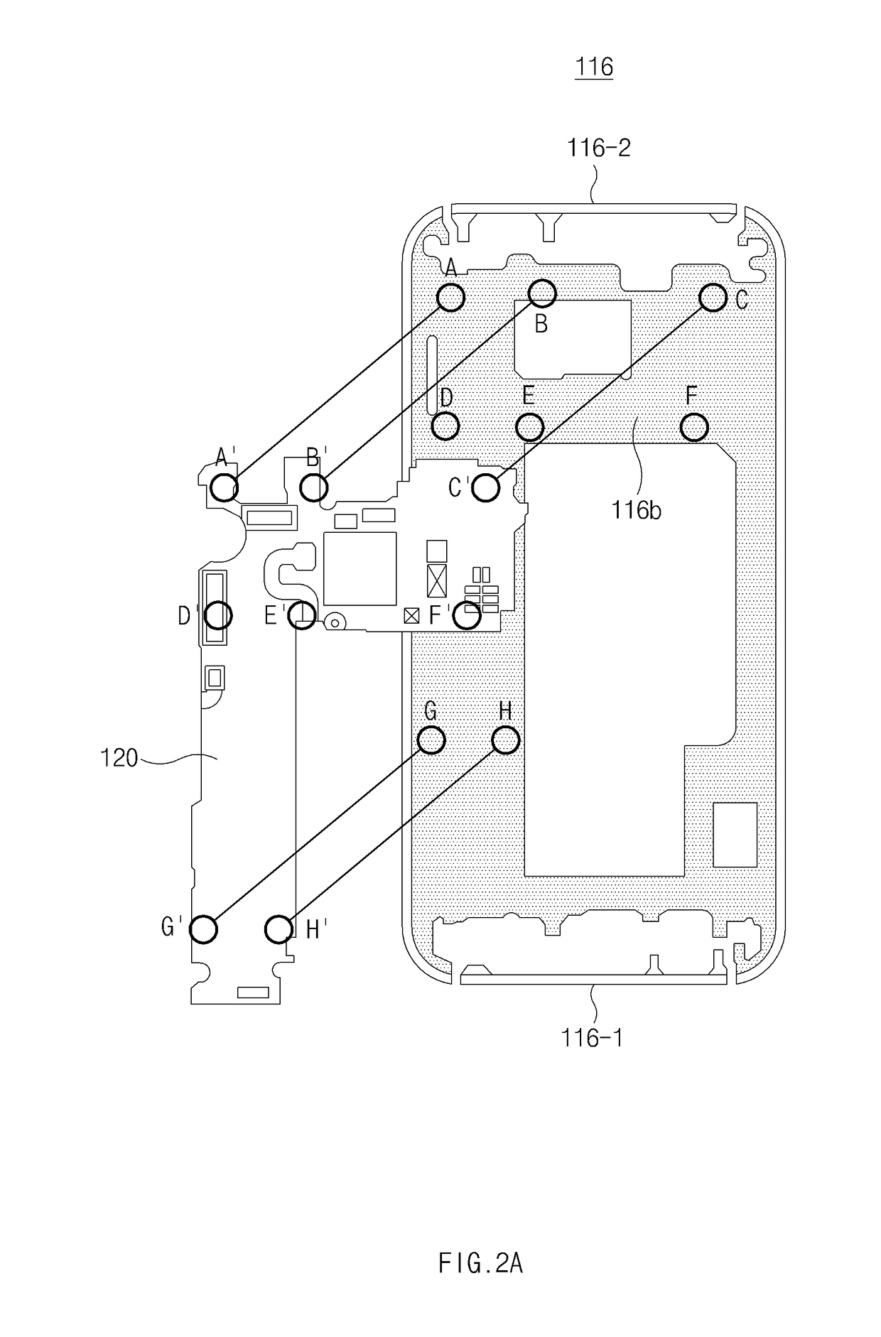
[0005]The disclosure has been made to address at least the disadvantages described above and to provide at least the advantages described below. Accordingly, an aspect of the disclosure is to provide a method and an electronic device for reducing an influence of a parasitic current by dynamically changing ground points of a plurality of antennas.

Problems solved by technology

The parasitic current may cause a decrease in the rate at which the top antenna and the bottom antenna transmit / receive signals, making it nearly impossible or difficult for the electronic device to communicate with any other electronic device.

Method used


Image

  • Method and electronic device for dynamically changing ground points of a plurality of antennas of the electronic device
  • Method and electronic device for dynamically changing ground points of a plurality of antennas of the electronic device
  • Method and electronic device for dynamically changing ground points of a plurality of antennas of the electronic device

Examples


Embodiment Construction

[0031]Embodiments of the disclosure will be described herein below with reference to the accompanying drawings. However, the embodiments of the disclosure are not limited to the specific embodiments and should be construed as including all modifications, changes, equivalent devices and methods, and / or alternative embodiments of the present disclosure. In the description of the drawings, similar reference numerals are used for similar elements.

[0032]The terms “have,”“may have,”“include,” and “may include” as used herein indicate the presence of corresponding features (for example, elements such as numerical values, functions, operations, or parts), and do not preclude the presence of additional features.

[0033]The terms “A or B,”“at least one of A or / and B,” or “one or more of A or / and B” as used herein include all possible combinations of items enumerated with them. For example, “A or B,”“at least one of A and B,” or “at least one of A or B” means (1) including at least one A, (2) in...


PUM


Abstract

An electronic device is provided and includes a housing, a support member including a first ground region, a printed circuit board including a second ground region, a plurality of switches electrically connecting the first ground region and the second ground region, a first antenna element including at least a portion of a first edge of the housing and electrically connected with the first ground region of the support member, a second antenna element including at least a portion of a second edge of the housing and electrically connected with the second ground region of the printed circuit board, and a wireless communication circuit configured to transmit/receive in a first frequency band based on a first electrical path, transmit/receive in a second frequency band based on a second electrical path, set ON/OF states of the plurality of switches to a first arrangement and a second arrangement, wherein at least one switch of the plurality of switches is set to an ON state in each of the first arrangement and the second arrangement.

Description

CROSS-REFERENCE TO RELATED APPLICATION(S)[0001]This application is based on and claims priority under 35 U.S.C. § 119(a) to Korean Patent Application Serial No. 10-2017-0102872, which was filed on Aug. 14, 2017, in the Korean Intellectual Property Office, the entire disclosure of which is incorporated herein by reference.BACKGROUND1. Field[0002]The present disclosure relates, generally, to an electronic device including a plurality of antennas, and more particularly, to a method and electronic device for dynamically changing ground points of a plurality of antennas of the electronic device through switching.2. Description of Related Art[0003]An electronic device, which is equipped with an antenna, such as a smartphone, a wearable device, or the like are in high demand as mobile communication technologies develop. The electronic device may communicate with any other electronic device (e.g., a base station or a personal computer) through the antenna. The electronic device may communic...

Claims


Application Information

Patent Timeline
Patent Type & Authority Applications(United States)
IPC IPC(8): H04B1/00H01Q1/48H01Q5/378H01Q21/00
CPCH04B1/0064H01Q1/48H01Q5/378H01Q21/0025H01Q1/22H01Q1/44H01Q1/50H01Q21/30H01Q1/243H01Q1/38H01Q9/0421H01Q21/28H04B1/3838H01Q5/30H01Q5/371H01Q9/0442H04B1/38
Inventor SEO, MIN CHEOLYUN, HIM CHANNAM, HO JUNGBYUN, JOON HOLEE, YOON JAELEE, JONG HYUCK
Owner SAMSUNG ELECTRONICS CO LTD
Why Eureka
Try Eureka