
Organic light emitting display device

a light-emitting display and organic technology, applied in the direction of static indicating devices, identification means, instruments, etc., can solve the problems of difficult to realize a desired quality image, high sensing time, complex pixel structure, etc., and achieve the effect of reducing the physical size of the sensing uni

Active Publication Date: 2018-04-26
LG DISPLAY CO LTD
View PDF0 Cites 43 Cited by
  • Summary
  • Abstract
  • Description
  • Claims
  • Application Information

AI Technical Summary

Benefits of technology

The present invention is about reducing the size of a sensing unit in display devices that detects the characteristics of driving TFTs. This is done by using a new structure that reduces the influence of noise, and can change the operation mode of detecting the driving TFTs. By doing this, the number of amplifiers and scalers in the sensing unit is reduced, reducing the size and cost of the source IC. Additionally, differential amplification is used to detect the characteristics of the driving TFTs while reducing the influence of noise mixed in the current on the sensing line.

Problems solved by technology

Unless the characteristic deviations are compensated, it is difficult to realize a desired quality image.
An external compensation method senses a characteristic parameter of the driving TFT for each pixel and adjusts input data according to a sensing value to precisely compensate the luminance deviation among pixels, but is disadvantageous in that it takes much time for sensing.
On the other hand, an internal compensation method can compensate the luminance deviation in real time, but has a disadvantage in that the pixel structure is complex and an aperture ratio is low.

Method used


Image

  • Organic light emitting display device
  • Organic light emitting display device
  • Organic light emitting display device

Examples


Embodiment Construction

[0041]Hereinafter, preferred embodiments of the present invention will be described in detail with reference to the accompanying drawings. Same reference numerals throughout the specification denote substantially identical components. In the following description, a detailed description of known functions and configurations incorporated herein will be omitted when it may make the subject matter of the present invention rather unclear. The term ‘may’ encompasses the full meanings of the term ‘can’.

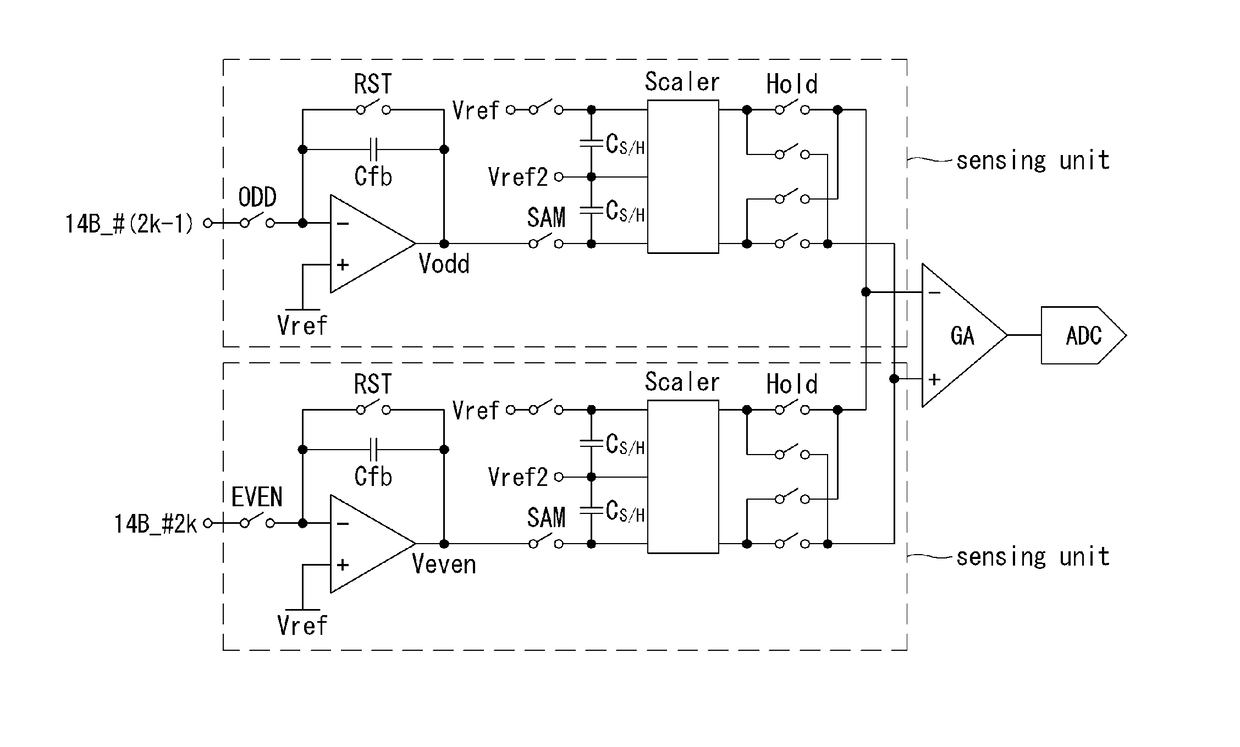
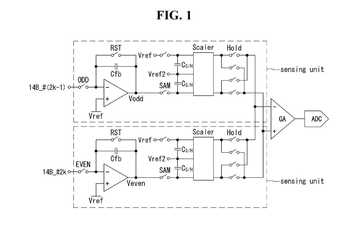
[0042]FIG. 1 shows a conventional sensing circuit configuration for detecting the characteristics of a pixel using a current.

[0043]When detecting the driving characteristics of a pixel by using a current, noise is a problem and a solution for solving the problem is indispensable. The sensing circuit in FIG. 1 is configured to differentially amplify the sensing values of two neighboring sensing lines by applying a correlated double sampling (CDS) method to reduce noise.

[0044]The CDS method s...


PUM


Abstract

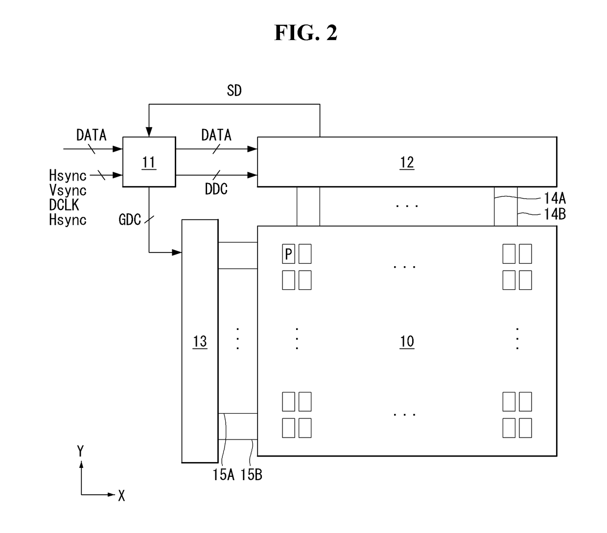
An organic light emitting display device in an embodiment of the present invention comprises a display panel equipped with a plurality of pixels each including an OLED and a driving TFT for driving the OLED and a sensing circuit connected to pixels through a sensing line and detecting driving characteristics of a corresponding pixel. The sensing circuit may comprise a plural sensing units including an integrator for integrating currents respectively flowing two adjacent sensing lines connected to inverting and non-inverting input terminals of a fully differential amplifier, a sampling unit for respectively sampling two integral outputs of the integrator and a scaler for regulating an operating range of outputs of the sampling unit, a differential amplifier for differentially amplifying one or more outputs of the scaler, and an ADC for converting an output of the differential amplifier into a digital sensing value.

Description

CROSS-REFERENCE TO RELATED APPLICATIONS[0001]This application claims the benefit of priority under 35 U.S.C. § 119(a) to Korean Patent Application No. 10-2016-0139528 filed on Oct. 25, 2016, which is incorporated by reference herein in its entirety into the present application.BACKGROUNDField[0002]The present invention relates to an organic light emitting display device for improving the structure of a sensing unit for detecting the electrical characteristics of a driving thin film transistor (TFT) for driving an organic light emitting pixel.Related Art[0003]An active matrix type organic light emitting display covers an organic light emitting diode (OLED) which emits light by itself, and has advantages of a fast response speed, high light emitting efficiency, high brightness, and a wide viewing angle.[0004]The organic light emitting display device arranges pixels each including an organic light emitting diode OLED and a driving TFT in a matrix form and adjusts the luminance of an im...

Claims


Application Information

Patent Timeline
Patent Type & Authority Applications(United States)
IPC IPC(8): H01L27/32H01L51/50G09F9/30H05B33/22H05B33/28H05B33/02G06K9/00H01L51/52H01L51/56H10K99/00
CPCH01L27/32H01L51/50G09F9/30H05B33/22H05B33/28H05B33/02G06K9/00013H01L51/5203H01L51/56G09G3/006G09G3/3225G09G2310/0291H10K59/131G09G3/3233G09G3/3291G09G2320/0295G06V40/1318H10K71/70G09G3/3275G09G2300/0828G09G2230/00H10K50/00H10K50/805H10K59/00H10K59/12H10K71/00
Inventor LEE, TAEYOUNGLEE, CHANGWOODO, OSUNG
Owner LG DISPLAY CO LTD
Learn More