Manufacturing method for a micromechanical device including an inclined optical window and corresponding micromechanical device

a micromechanical device and optical window technology, applied in the direction of optical elements, fluid speed measurement, instruments, etc., can solve the problems of interference, high cost of three-dimensional structure manufacturing methods, and inability to yield the necessary optical quality, etc., to achieve the effect of easy and precise manufacturing of the flap area

Inactive Publication Date: 2018-03-08
ROBERT BOSCH GMBH
View PDF1 Cites 3 Cited by
  • Summary
  • Abstract
  • Description
  • Claims
  • Application Information

AI Technical Summary

Benefits of technology

[0020]According to another refinement, the recess is formed as a second cavity which extends starting from the back side toward a second diaphragm area on the front side of the first substrate, the flap area being formed by structuring the second diaphragm area. This makes it possible for the third wafer substrate to be dispensed with.
[0021]According to another refinement, the first substrate and the second substrate are wafer substrat...

Problems solved by technology

When the stationary reflections of a micromechanical micromirror scanning device are located in the scanning area of the micromirror, their intensity exceeds that of the projected image and is perceived as interference.
The methods by which the three-dimensional structures ar...

Method used


Image

  • Manufacturing method for a micromechanical device including an inclined optical window and corresponding micromechanical device
  • Manufacturing method for a micromechanical device including an inclined optical window and corresponding micromechanical device
  • Manufacturing method for a micromechanical device including an inclined optical window and corresponding micromechanical device

Examples


Embodiment Construction

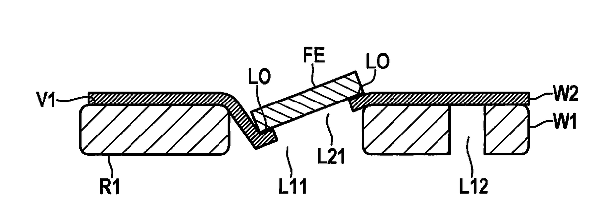
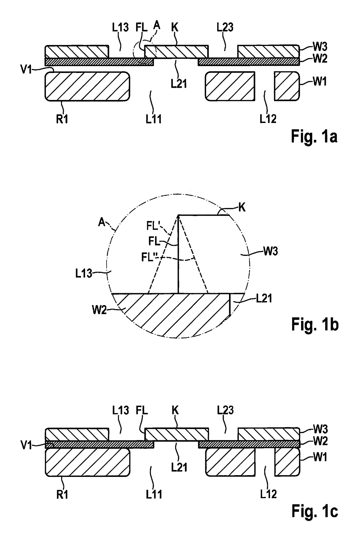
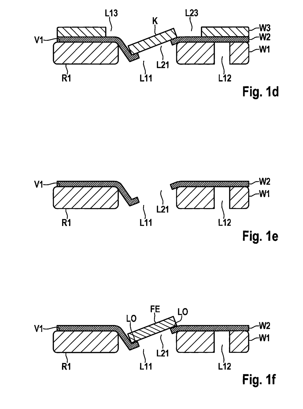
[0032]FIGS. 1a through 1f are schematic cross-sectional illustrations for elucidating a manufacturing method for a micromechanical device including an inclined optical window and a corresponding micromechanical device according to a first specific embodiment of the present invention.

[0033]The micromechanical device including the inclined optical window according to the first specific embodiment is usable, for example, as a protective wafer device for a micromechanical micromirror scanning device.

[0034]The manufacture of the micromechanical device is described on the wafer level, although it is not limited thereto and could also take place on the component level. For simplifying the illustration, only the manufacture of a single inclined optical window is shown, although a plurality of inclined optical windows could be produced on the wafer level.

[0035]In FIG. 1a, reference numeral W1 indicates a first wafer substrate, for example a silicon wafer substrate, W2 indicates a second wafe...


PUM

PropertyMeasurementUnit
Areaaaaaaaaaaa
Deformation enthalpyaaaaaaaaaa

Abstract

A manufacturing method for a micromechanical device including an inclined optical window and a corresponding micromechanical device. The method includes: providing a first substrate having front and back sides and a recess; applying a second substrate on the front side, the second substrate being thermally deformable and having a first through hole above the recess which has a smaller lateral extension than the recess; forming a flap area on the second substrate above/below the first through hole which is situated in a first position with respect to the first substrate; thermally deforming the second substrate, the flap area being moved into a second position within the recess which is inclined with respect to the first position and optionally subsided into the recess; removing the flap area from the second substrate; and attaching the optical window on the second substrate above/below the first through hole in the second inclined position.

Description

RELATED APPLICATION INFORMATION[0001]The present application claims priority to and the benefit of German patent application no. 10 2016 216 918.1, which was filed in Germany on Sep. 7, 2016, the disclosure of which is incorporated herein by reference.FIELD OF THE INVENTION[0002]The present invention relates to a manufacturing method for a micromechanical device including an inclined optical window and a corresponding micromechanical device.BACKGROUND INFORMATION[0003]Although it is also possible to use arbitrary optical devices and systems, the present invention and the underlying object are explained based on optical micromechanical micromirror scanning devices.[0004]Micromechanical MEMS components must be protected against harmful external environmental influences (e.g., wet, aggressive media, etc.) for their protection. It is also necessary to protect the components against mechanical contact / destruction as well as to allow them to be separated from a wafer composite into chips ...

Claims


Application Information

Patent Timeline
IPC IPC(8): B81C1/00B81B7/00G02B27/00
CPCB81C1/00626B81B7/0058G02B26/0833B81C2201/0116B81B2201/042G02B27/0006B81B7/0009B81B7/02B81C1/00634B81C3/001B81C1/00317B81B2203/0384
Inventor STEUER, BENJAMINPINTER, STEFAN
Owner ROBERT BOSCH GMBH
Why Eureka
Try Eureka