Solid-state imaging device, manufacturing method of solid-state imaging device, and imaging system
- Summary
- Abstract
- Description
- Claims
- Application Information
AI Technical Summary
Benefits of technology
Problems solved by technology
Method used
Image

Examples
first embodiment
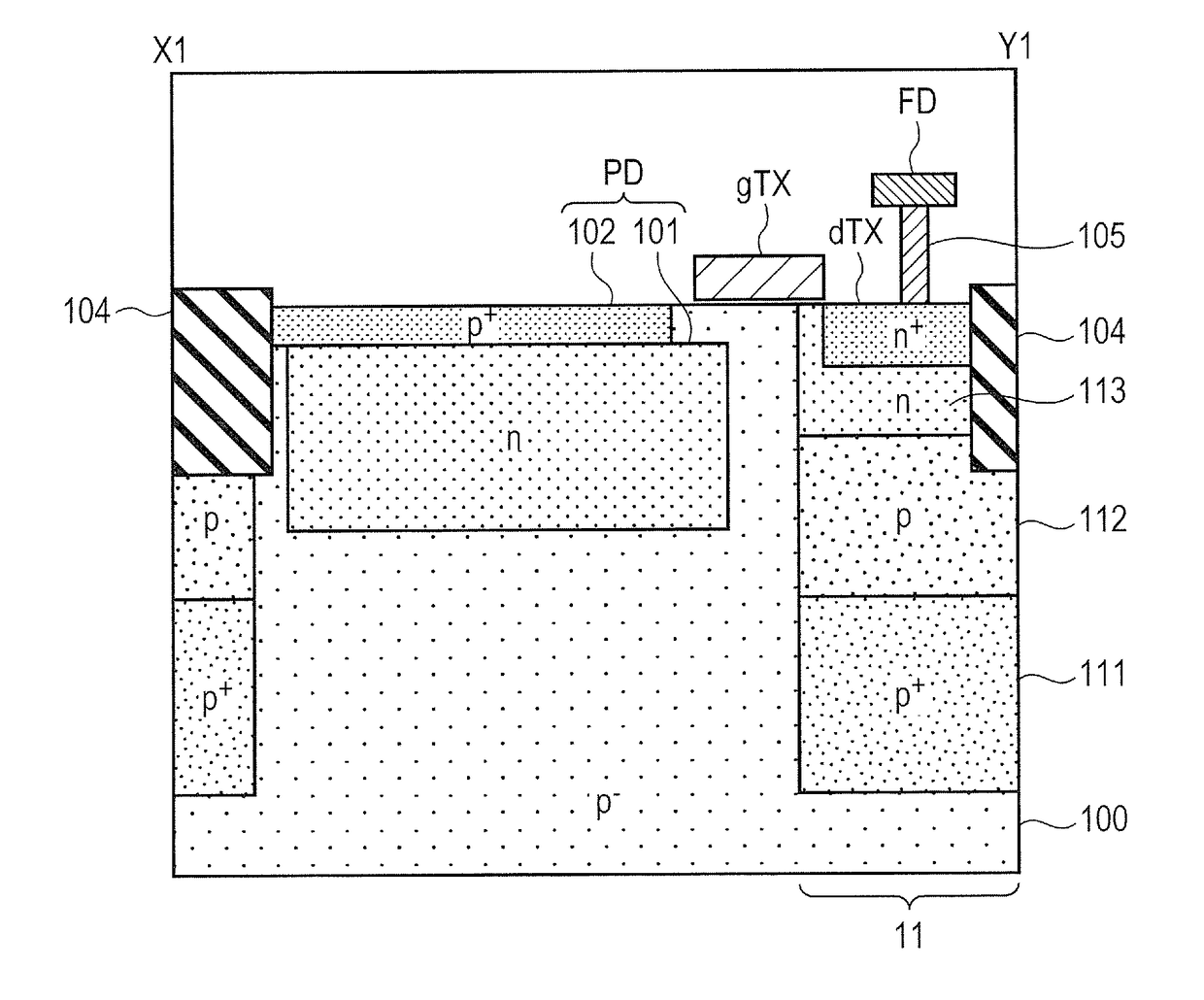
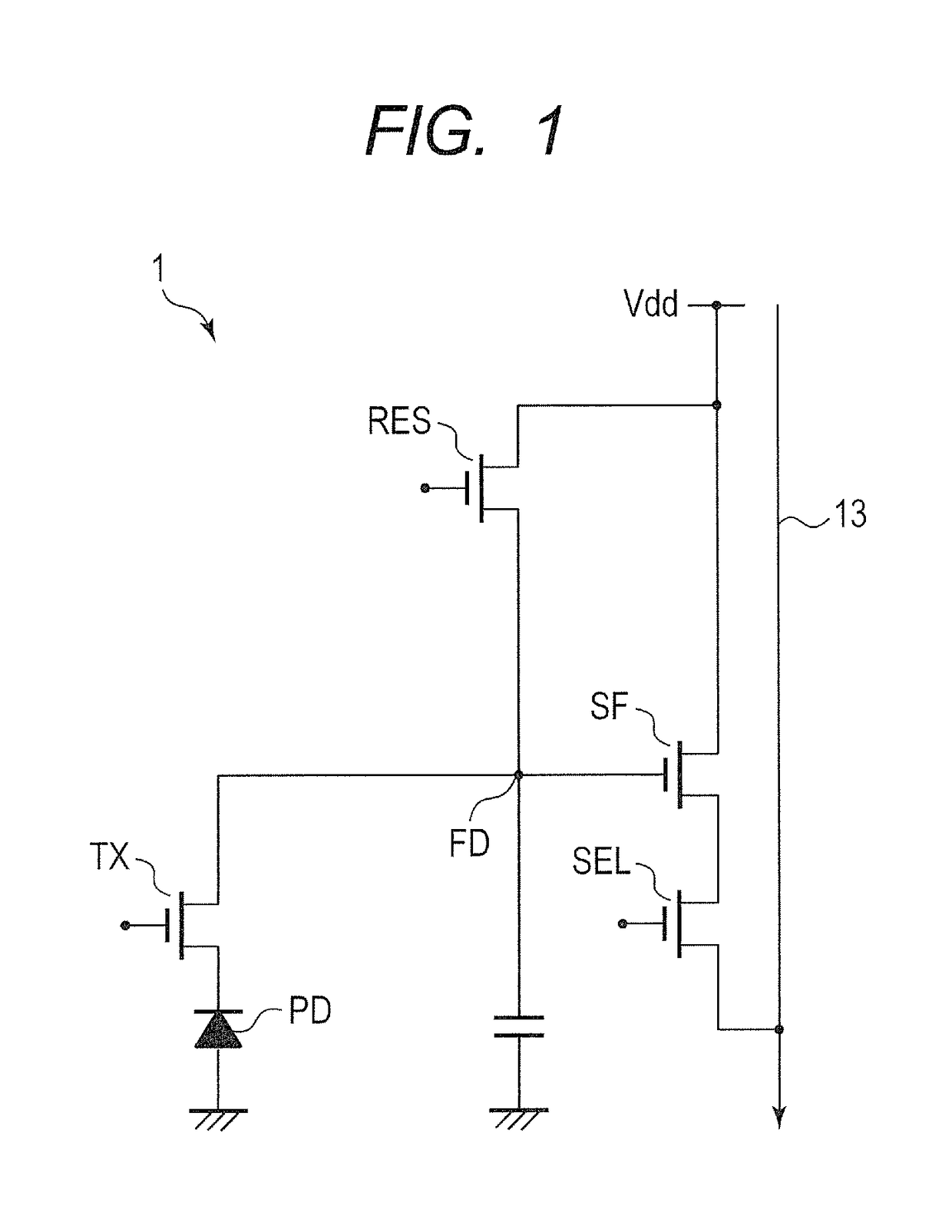
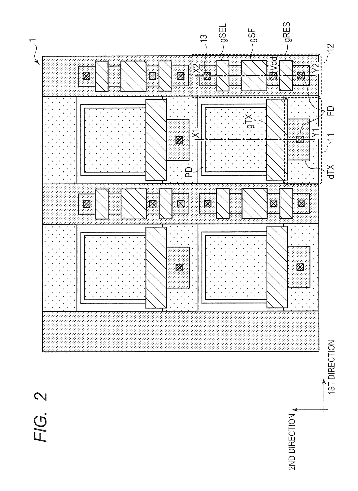
[0022]A solid-state imaging device according to the first embodiment will be described with reference to FIGS. 1 to 5. FIG. 1 is a schematic diagram illustrating an equivalent circuit of a pixel 1 in the solid-state imaging device according to the first embodiment.
[0023]The pixel 1 of the embodiment illustrated in FIG. has a photoelectric conversion unit PD, a transfer transistor TX, an amplifier transistor SF, a reset transistor RES, and a select transistor SEL. The transfer transistor TX, reset transistor RES, and select transistor SEL are controlled by control signals which are output from a vertical scanning circuit (not shown). It is sufficient that the pixel 1 of the embodiment has at least the photoelectric conversion unit PD and transfer transistor TX and there is also a case where the other transistors are omitted. In the following description, there is a case where the amplifier transistor SF, select transistor SEL, and reset transistor RES are collectively called an outpu...
second embodiment
[0051]Subsequently, a solid-state imaging device according to the second embodiment will be described with reference to FIGS. 6 to 8. The first embodiment has been described with respect to a construction in which one pixel 1 has one photoelectric conversion unit PD. On the other hand, the present embodiment will be described with respect to a construction in which one pixel 1 has two photoelectric conversion units. A construction different from the first embodiment will be mainly described hereinbelow.
[0052]FIG. 6 is a schematic diagram illustrating an equivalent circuit of a pixel 1b in the solid-state imaging device according to the second embodiment. The pixel 1b of the present embodiment illustrated in FIG. 6 differs from the pixel 1 illustrated in FIG. 1 mainly with respect to a point that the pixel 1b has two photoelectric conversion units PD1 and PD2. In other words, the pixel 1b of the present embodiment has a construction in which the two photoelectric conversion units PD1...
third embodiment
[0062]Subsequently, a solid-state imaging device according to the third embodiment will be described with reference to FIGS. 9 to 11. In the present embodiment, a plurality of photoelectric conversion units are line-symmetrically arranged to an axis of symmetry which passes through the common drain region dTX. A construction different from the second embodiment will be mainly described hereinbelow.
[0063]FIG. 9 is a schematic diagram illustrating an equivalent circuit of a pixel 1c in the solid-state imaging device according to the third embodiment. The pixel 1c of the present embodiment illustrated in FIG. 9 differs mainly from the pixel 1b illustrated in FIG. 6 with respect to a point that the pixel 1c has four photoelectric conversion units PD1 to PD4. In other words, the pixel 1c of the present embodiment has a construction in which the four photoelectric conversion units PD1 to PD4 share one floating diffusion unit FD. The pixel 1c of the present embodiment has transfer transist...
PUM
 Abstract
Description
Claims
Application Information
 - R&D
- Intellectual Property
- Life Sciences
- Materials
- Tech Scout
- Unparalleled Data Quality
- Higher Quality Content
- 60% Fewer Hallucinations
Browse by: Latest US Patents, China's latest patents, Technical Efficacy Thesaurus, Application Domain, Technology Topic, Popular Technical Reports.
© 2025 PatSnap. All rights reserved.Legal|Privacy policy|Modern Slavery Act Transparency Statement|Sitemap|About US| Contact US: help@patsnap.com