Display device and electronic device

Active Publication Date: 2017-12-28
SEMICON ENERGY LAB CO LTD
View PDF8 Cites 17 Cited by
  • Summary
  • Abstract
  • Description
  • Claims
  • Application Information

AI Technical Summary

Benefits of technology

The patent text describes a display device that is smaller in size and has high quality, reliability, low power consumption, shock resistance, and high producibility. The device includes a flexible display with a small radius of curvature, which can cause short-circuit or disconnection of wiring or electrode. To solve this problem, the patent proposes a display device with multiple display regions between two flexible substrates, which can provide high display quality, reliability, low power consumption, shock resistance, non-breakability, lightweight, and high producibility.

Problems solved by technology

Therefore, a decrease in the radius of curvature of the bend portion causes a short-circuit or a disconnection of the wiring or electrode included in the bend portion, easily leading to problems such as defective operation and lowered reliability.
In particular, a decrease in the power consumption of a display device is demanded of devices using batteries as power sources, such as mobile phones, smartphones, tablet terminals, smart watches, and notebook personal computers, because the proportion of the power consumption of the display device to the total power consumption is large.
When a portable electronic device is dropped or put in a trouser pocket or the like, its display device might be cracked in some cases.

Method used


Image

  • Display device and electronic device
  • Display device and electronic device
  • Display device and electronic device

Examples


embodiment 1

[0091]In this embodiment, a display device of one embodiment of the present invention will be described with reference to drawings.

100>

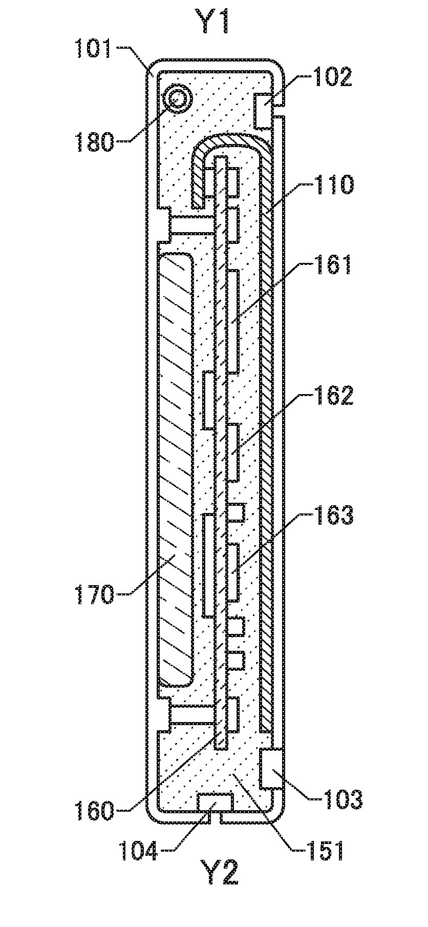
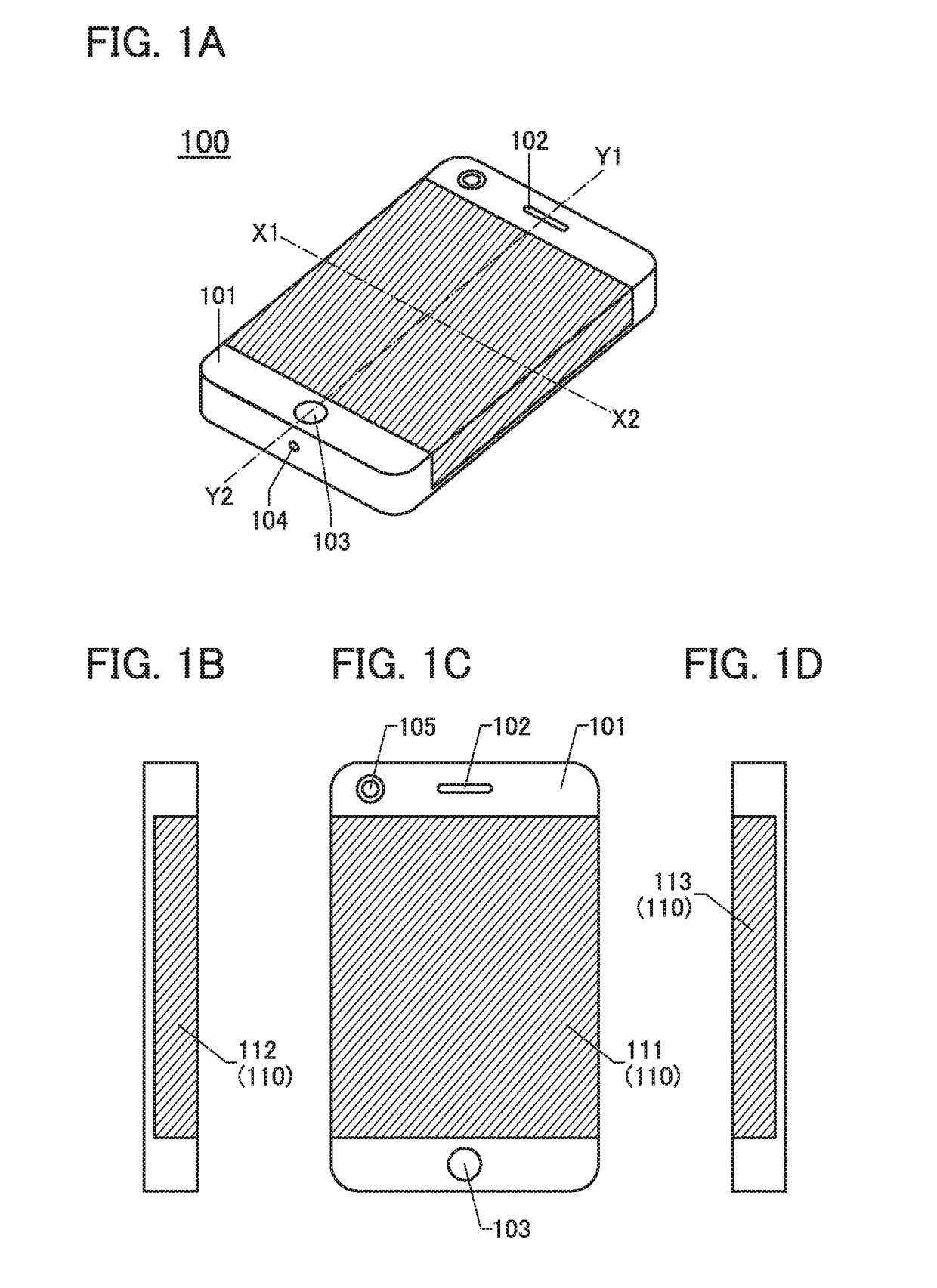
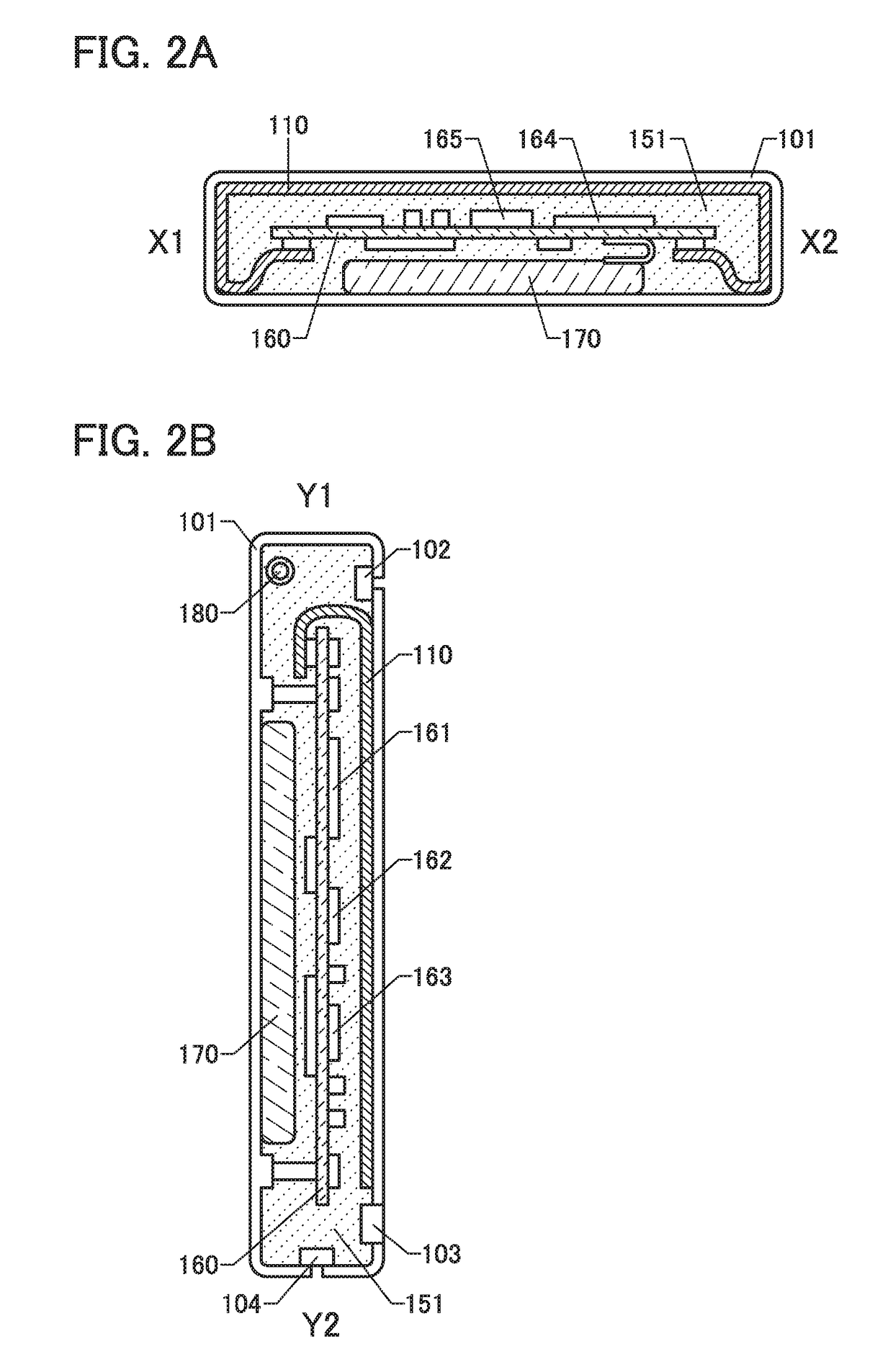
[0092]FIG. 1A is a perspective view of a portable electronic device 100 including the display device of one embodiment of the present invention. FIG. 1B is a left side view of the electronic device 100. FIG. 1C is a front view of the electronic device 100. FIG. 1D is a right side view of the electronic device 100. FIG. 2A is a cross-sectional view of a portion indicated by dashed-dotted line X1-X2 in FIG. 1A. FIG. 2B is a cross-sectional view of a portion indicated by dashed-dotted line Y1-Y2 in FIG. 1A.

[0093]The electronic device 100 includes a housing 101, an audio output device 102, an operation switch 103, an audio input device 104, an imaging device 105, a display device 110, and the like. The display device 110 includes a display region 111 overlapping with the front of the electronic device 100, a display region 112 overlapping with the left s...

embodiment 2

[0158]In this embodiment, more specific configuration examples of the display device 110 of one embodiment of the present invention will be described.

[0159]FIG. 6A is a block diagram illustrating a configuration example of the display device 110. The display device 110 may include a circuit 232a between the input terminal 121 and the display region 111, a circuit 233a between the input terminal 121 and the display region 111, a circuit 232b between the input terminal 122 and the display region 112, a circuit 233b between the input terminal 122 and the display region 112, a circuit 232c between the input terminal 123 and the display region 113, and a circuit 233c between the input terminal 123 and the display region 113.

[0160]The circuit 232a, the circuit 232b, and the circuit 232c may each function as, for example, a scan line driver circuit. The circuit 233a, the circuit 233b, and the circuit 233c may each function as, for example, a signal line driver circuit. In some cases, the c...

configuration example 1

[0164]FIG. 6B is a block diagram illustrating a configuration example of the display region 111, the circuit 232a, and the circuit 233a.

[0165]The display region 111 includes m wirings 235 and n wirings 236. The m wirings 235 are arranged substantially parallel to each other, and potentials thereof are controlled by the circuit 232a. The n wirings 236 are arranged substantially parallel to each other, and potentials thereof are controlled by the circuit 233a. The display region 111 includes the plurality of pixels 230 arranged in a matrix.

[0166]Each of the wirings 235 is electrically connected to the n pixels 230 in the corresponding row among the pixels 230 arranged in m rows and n columns in the display region 111. Each of the wirings 236 is electrically connected to the m pixels 230 in the corresponding column among the pixels 230 arranged in the m rows and the n columns. Note that m and n are each an integer of 1 or more.

[0167]The pixel 230 includes a pixel circuit 237 and a dis...


PUM


Abstract

A highly reliable display device is provided. In a flexible display device including at least a first display region and a second display region, at least a portion of a wiring provided in the first display region or the second display region has a meandering shape or a chain-like shape. Since the wiring has a meandering shape or a chain-like shape, a short-circuit, a disconnection, or the like of the wiring due to curving or bending of the display device does not occur easily. The wiring having a meandering shape or a chain-like shape can prevent defective operation, lowered reliability, or the like of the display device.

Description

BACKGROUND OF THE INVENTION1. Field of the Invention[0001]One embodiment of the present invention relates to an object, a method, or a manufacturing method. One embodiment of the present invention relates to a process, a machine, manufacture, or a composition of matter. One embodiment of the present invention relates to a semiconductor device, a display device, a light-emitting device, a lighting device, a power storage device, a memory device, a processor, a driving method thereof, or a manufacturing method thereof.[0002]In this specification and the like, the term “semiconductor device” means all devices which can operate by utilizing semiconductor characteristics. For example, semiconductor elements (such as a diode and a transistor), semiconductor circuits, and the like are regarded as semiconductor devices. A display device, a light-emitting device, a lighting device, a photoelectric conversion device, a memory device, an imaging device, an electronic device, and the like may i...

Claims


Application Information

Patent Timeline
IPC IPC(8): G02F1/1347H01L27/32G02F1/1333
CPCG02F1/1347G02F1/133305G02F1/133308G02F2001/13478G02F2201/44G02F2203/02H01L27/3232G02F1/133553G02F1/136286H10K59/50H10K59/131H10K2102/311G02F1/13478
Inventor YAMAZAKI, SHUNPEIKUBOTA, DAISUKEUOCHI, HIDEKI
Owner SEMICON ENERGY LAB CO LTD
Why Eureka
Try Eureka