Thin-film bulk acoustic resonator, semiconductor apparatus comprising of such an acoustic resonator, and manufacture thereof
a technology of acoustic resonators and thin films, which is applied in the direction of electrical devices, impedence networks, and semiconductor devices. it can solve the problems of weakening the integrity of the lower and adversely affecting the performance of the fbar, and achieve the effect of improving the resonance performan
- Summary
- Abstract
- Description
- Claims
- Application Information
AI Technical Summary
Benefits of technology
Problems solved by technology
Method used
Image
Examples
first embodiment
A First Embodiment
[0114]FIGS. 2A and 2B illustrate an FBAR device in accordance with one of the embodiments of the present disclosure. FIG. 2A shows a schematic cross-sectional view of such an FBAR device; FIG. 2B shows a plan view of FIG. 2A.
[0115]As illustrated in FIG. 2A, the FBAR device 200 may include the following elements: a lower dielectric layer 201, wherein there is a first cavity 203 inside the lower dielectric layer 201. As illustrated in FIG. 2B, the plan view of the first cavity 203 is a first polygon 2030, the first polygon 2030 has at least one pair of parallel sides to facilitate the measurement and control during the micro-fabrication process. The first cavity 203 may have exactly same profiles in thickness direction.
[0116]The plan view in FIG. 2B is obtained by observing the corresponding element in the schematic diagram of FIG. 2A in a thickness direction from the “top” of FIG. 2A. In this application, the “plan view” of an element in a schematic diagram refers t...
second embodiment
A Second Embodiment
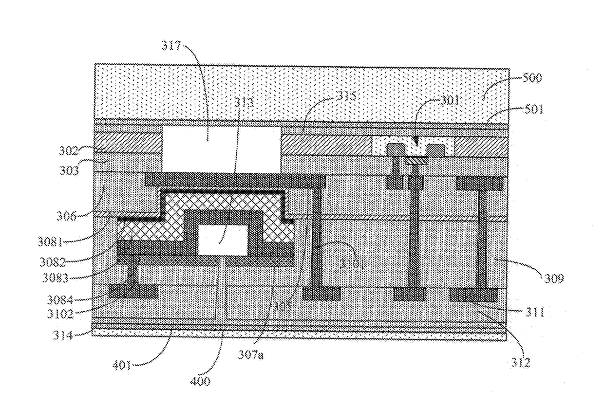
[0138]Referring to FIG. 3Q and FIG. 3S1, one embodiment of the semiconductor apparatus in this inventive concept is presented.
[0139]Referring to FIG. 3Q, as an example, the semiconductor apparatus of the inventive concept may include an isolation trench layer 302 and a first dielectric layer 303 on the isolation trench layer 302. The isolation trench layer 302 may be filled with a filling material such as silicon-based oxide, nitride, or oxynitride.
[0140]The first dielectric layer 303 may be made of materials such as silicon-based oxide or nitride. For example, the material can be silicon dioxide (SiO2), carbon-fluorine compound (CF), carbon-doped silicon oxide (SiOC), silicon nitride (SiN), or silicon carbonitride (SiCN). Alternatively, the first dielectric layer 303 may also be made of carbon-fluorine compounds comprising silicon carbonitride (SiCN) film. The major components of the carbon-fluorine compound are fluorine (F) and carbon (C). The carbon-fluorine co...
PUM
| Property | Measurement | Unit |
|---|---|---|
| thickness | aaaaa | aaaaa |
| shape | aaaaa | aaaaa |
| piezoelectric | aaaaa | aaaaa |
Abstract
Description
Claims
Application Information
 - R&D
- Intellectual Property
- Life Sciences
- Materials
- Tech Scout
- Unparalleled Data Quality
- Higher Quality Content
- 60% Fewer Hallucinations
Browse by: Latest US Patents, China's latest patents, Technical Efficacy Thesaurus, Application Domain, Technology Topic, Popular Technical Reports.
© 2025 PatSnap. All rights reserved.Legal|Privacy policy|Modern Slavery Act Transparency Statement|Sitemap|About US| Contact US: help@patsnap.com


