Ltps array substrate and manufactoring method thereof
- Summary
- Abstract
- Description
- Claims
- Application Information
AI Technical Summary
Benefits of technology
Problems solved by technology
Method used
Image

Examples
Embodiment Construction
[0027]The following will combine the drawings of the embodiment of the present invention to clearly and completely describe the technical solution of the exemplary embodiments provided by the present invention.
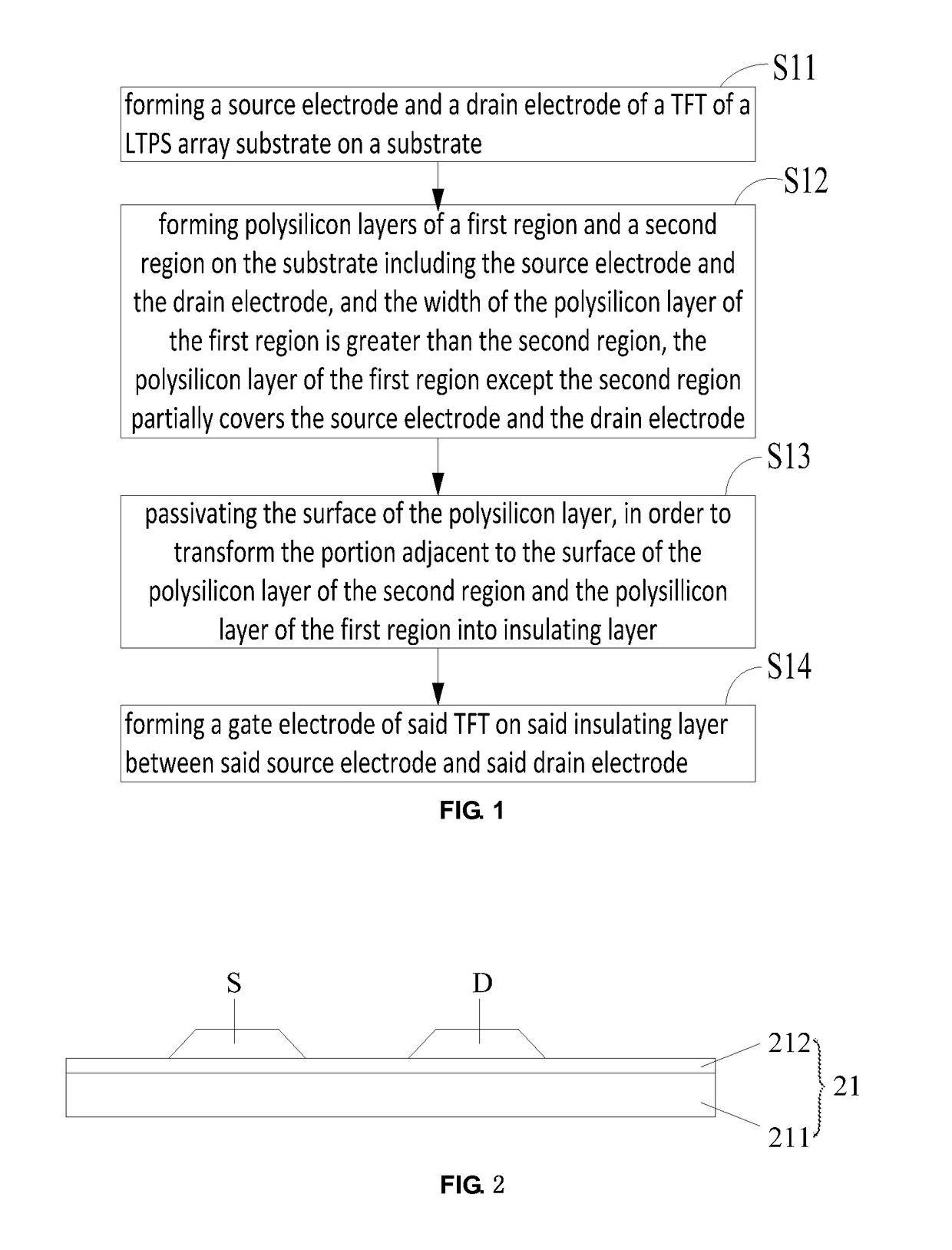
[0028]FIG. 1 is a flow chart of a manufacturing method of a LTPS array substrate of an embodiment of the present invention. As shown in FIG. 1, the manufacturing method of the present invention comprises the following steps:
[0029]Step 11: forming a source electrode and a drain electrode of a TFT of said LTPS array substrate on a substrate.
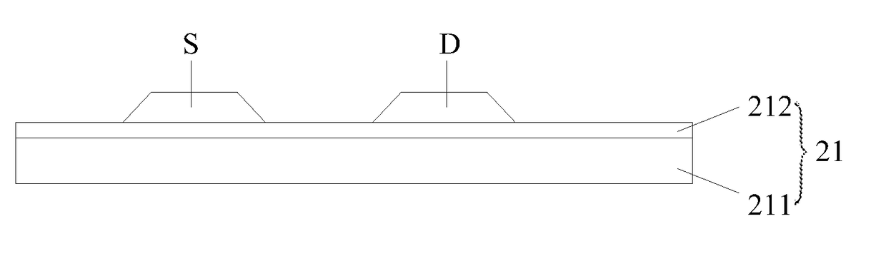
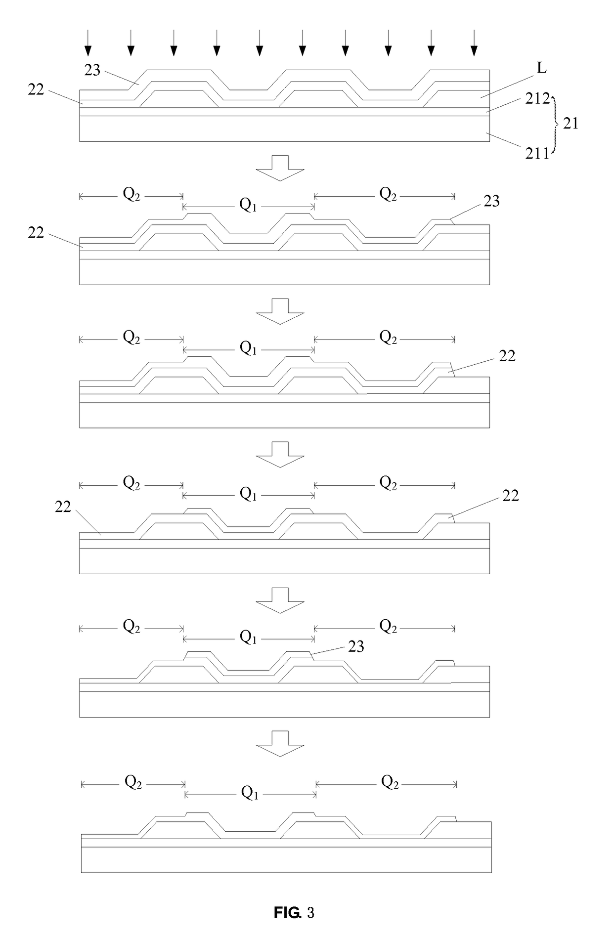
[0030]The substrate is used to form a LTPS array substrate of the liquid crystal display panel, which could be a glass substrate, a plastic substrate or a flexible substrate. As shown in FIG. 2, the substrate 21 could also comprise a backing plate 211 and a transparent buffer layer 212 forming on the backing plate 211. Wherein the buffer layer 212 is SiNx layer, SiOx layer or the combination of both, the buffer layer 212 is used to prevent th...
PUM
 Abstract
Description
Claims
Application Information
 - R&D
- Intellectual Property
- Life Sciences
- Materials
- Tech Scout
- Unparalleled Data Quality
- Higher Quality Content
- 60% Fewer Hallucinations
Browse by: Latest US Patents, China's latest patents, Technical Efficacy Thesaurus, Application Domain, Technology Topic, Popular Technical Reports.
© 2025 PatSnap. All rights reserved.Legal|Privacy policy|Modern Slavery Act Transparency Statement|Sitemap|About US| Contact US: help@patsnap.com