
Silicon core wire for producing polycrystalline silicon rod, and device for producing polycrystalline silicon rod

a technology of polycrystalline silicon and core wire, which is applied in the direction of chemical/physical/physical-chemical processes, inorganic chemistry, chemical/physical/physical-chemical processes, etc., can solve the problems of complex structure of holding member (graphite chuck), remarkably reduced mutual connection strength, and silicon core wire falling. , to achieve the effect of preventing the failure of silicon core wire and reducing contact resistan

Inactive Publication Date: 2017-06-08
SHIN ETSU CHEM IND CO LTD
View PDF0 Cites 1 Cited by
  • Summary
  • Abstract
  • Description
  • Claims
  • Application Information

AI Technical Summary

Benefits of technology

The present invention is designed to prevent failure and minimize damage during the process of depositing polycrystalline silicon onto a silicon core wire. This is achieved by using a holding member with tapers that allows the wire to be securely positioned without needing an external force. The contact between the silicon core wire and the holding member is achieved through the weight of the wire, reducing the likelihood of sparks and failures.

Problems solved by technology

When sparks and the like are thus generated, the silicon core wire is locally fused, undergoes structural damage, and otherwise, whereby the mutual connection strength remarkably decreases and in the worst case, the silicon core wire falls, failures or otherwise in the early stage of the deposition reaction.
The inventions disclosed in the above Patent Literatures 2 to 4, however, have the following drawbacks: the structure of the holding member (graphite chuck) is complex and the time required for setting work is long, and also slight loosening, offset excessive fastening and the like of the screw to fix the holding member make a locally excessive current to flow and bring about easy generation of sparks.
The electrode disclosed in Patent Literature 5, however, cannot help becoming expensive because of the complexity of the electrode shape, and additionally, the Patent Literature 5 makes no reference to how a contact portion of the electrode with the filament rod is devised, which is most important for prevention of falling and the like in the early deposition period of a polycrystalline silicon.
The chuck structure disclosed in the Patent Literature 7, however, has a high contact resistance between a groove provided at the front end part of the graphite-made chuck having its circularly conical-shaped upper part and the starter filament, and exhibits very high possibilities in failure and falling.
The clamping device disclosed in the Patent Literature 9, however, since having a complex clamping structure, cannot help being expensive.
The chuck structure disclosed in the Patent Literature 10, however, gives no consideration to shaking of the supported silicon core wire (filament) in the furnace, and is conceivably not suitable for production of polycrystalline silicon rods, whose diameters are being enlarged.

Method used


Image

  • Silicon core wire for producing polycrystalline silicon rod, and device for producing polycrystalline silicon rod
  • Silicon core wire for producing polycrystalline silicon rod, and device for producing polycrystalline silicon rod
  • Silicon core wire for producing polycrystalline silicon rod, and device for producing polycrystalline silicon rod

Examples


example 1

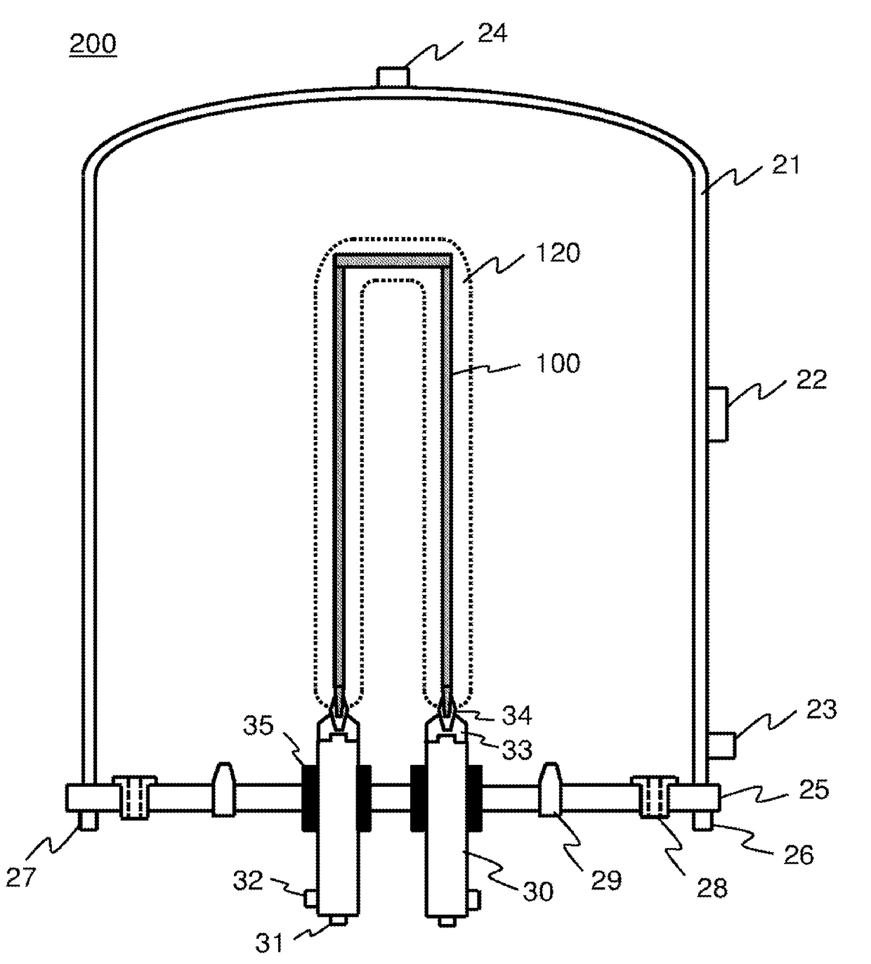
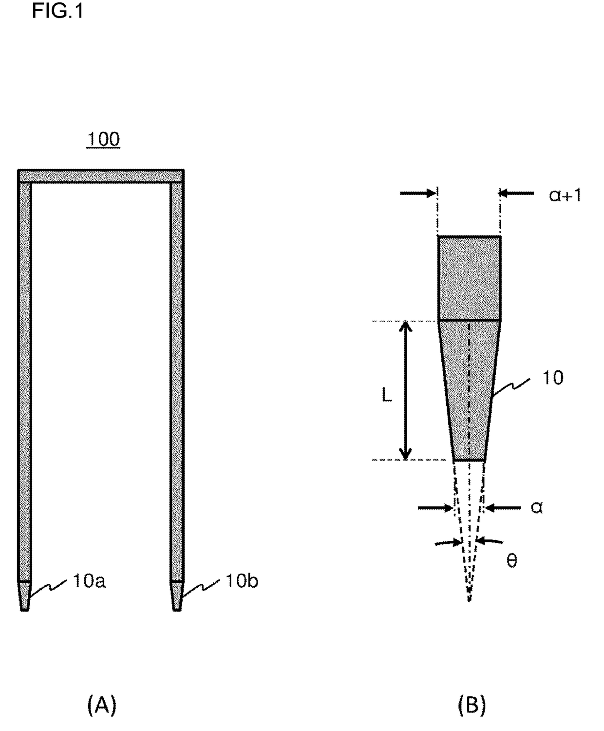
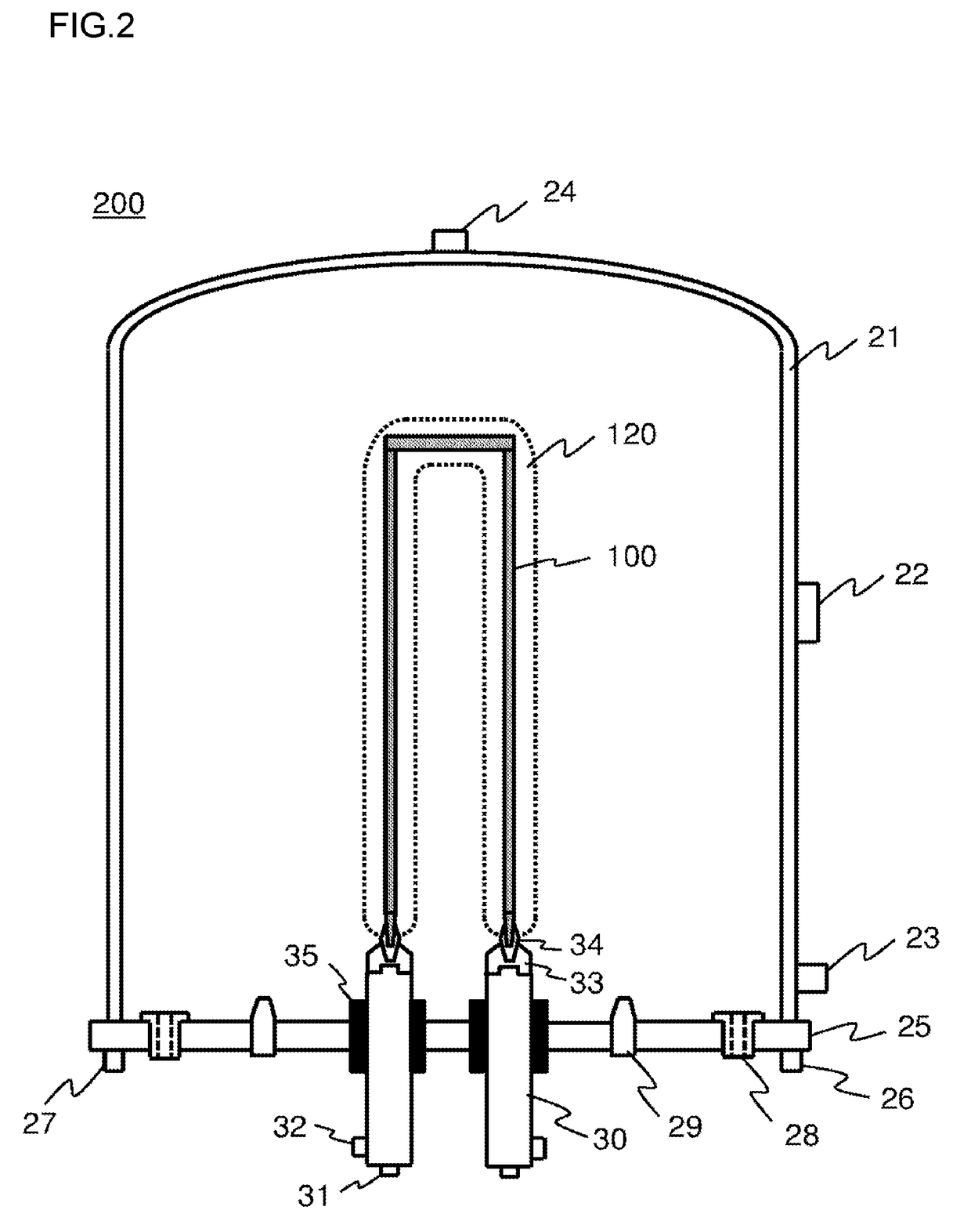
[0078]In the form illustrated in FIG. 3, a silicon core wire 100 was set in a reaction furnace 200. The height (length) of the silicon core wire 100 was 1,850 mm; and the cross-section had a rectangle whose one side was 7 mm. The end part 10 of the silicon core wire 100 was provided with a tapered part whose taper was 1 / 50 (taper angle: 1.1459°) and taper length was 45 mm.

[0079]The cross-section of an opening part of a core wire holder 34 to accommodate the end part 10 of the silicon core wire 100 was made to be a rectangle; the opening part is processed into a taper shape whose taper was 1 / 50 (taper angle: 1.1459°) and taper length was 40 mm; and the silicon core wire 100 resulted in being held by its own weight.

[0080]After the interior of the reaction furnace 200 was replaced by hydrogen, a voltage of 2,000 V was applied to the silicon core wire 100, which was thus energized (ignited). Thereafter, a raw material gas in which trichlorosilane was diluted with hydrogen was supplied i...

example 2

[0082]The production of 10 batches of a polycrystalline silicon rod 120 of 45 mm in diameter was carried out under the same condition as in Example 1, except for causing polycrystalline silicons to deposit at a deposition rate of 15 μm / min, and there were observed no local fusion of or structural damage to the silicon core wires due to generation of sparks and the like, and no falling nor failure of the silicon core wires 100.

example 3

[0087]In the form illustrated in FIG. 3, a silicon core wire 100 was set in a reaction furnace 200. The height (length) of the silicon core wire 100 was 2,000 mm; and the cross-section had a rectangle whose one side was 7 mm. The end part 10 of the silicon core wire 100 was provided with a tapered part whose taper was 1 / 50 (taper angle: 1.1459°) and taper length was 45 mm.

[0088]The cross-section of an opening part of a core wire holder 34 to accommodate the end part 10 of the silicon core wire 100 was made to be a rectangle; the opening part is processed into a taper shape whose taper was 1 / 50 (taper angle: 1.1459°) and taper length was 45 mm; and the silicon core wire 100 resulted in being held by its own weight.

[0089]After the interior of the reaction furnace 200 was replaced by hydrogen, a voltage of 2,000 V was applied to the silicon core wire 100, which was thus energized (ignited). Thereafter, a raw material gas in which trichlorosilane was diluted with hydrogen was supplied i...


PUM

PropertyMeasurementUnit
taper lengthaaaaaaaaaa
taper angleaaaaaaaaaa

Abstract

A core wire holder 34 (holding member) has a taper of a positive taper angle on the lower end part thereof. On the other hand, in an adaptor 33 (supporting member) to be used for connection of a metal electrode 30 with the core wire holder 34 (holding member) for energization of a silicon core wire 100, the inner surface of a hole of the adaptor 33 into which the lower end part of the core wire holder 34 (holding member) is inserted, when the opening side of the hole is set upward and the insertion direction of the lower end part of the holding member is set downward, has a taper of a positive taper angle. The lower end part of the core wire holder 34 (holding member) is inserted in the hole of the adaptor 33 (supporting member) and the silicon core wire 100 is thus fixed.

Description

TECHNICAL FIELD[0001]The present invention relates to a technology of producing a polycrystalline silicon rod, and particularly to a technology of making possible the stable production of the polycrystalline silicon rod by preventing failure, falling and the like of a silicon core wire when a polycrystalline silicon is deposited on the silicon core wire by a CVD reaction.BACKGROUND ART[0002]As production methods of polycrystalline silicons to become raw materials of single-crystal silicon substrates for semiconductor production and silicon substrates for solar cell production, there are known the Siemens process and the Union Carbide process.[0003]Needless to say, the Siemens process is a process in which a raw material gas containing a chlorosilane is contacted with a heated silicon core wire (silicon starter filament) to thereby cause a polycrystalline silicon to vapor-phase grow on a surface of the silicon core wire by a CVD reaction.[0004]The Union Carbide process is a process i...

Claims


Application Information

Patent Timeline
Patent Type & Authority Applications(United States)
IPC IPC(8): C01B33/035B01J19/08
CPCC01B33/035B01J2219/0879B01J2219/0803B01J19/087C01P2004/12
Inventor TANAKA, SHUJIOKADA, TETSURO
Owner SHIN ETSU CHEM IND CO LTD
Learn More