Semiconductor devices and methods of fabricating the same

a technology of semiconductor devices and semiconductors, applied in semiconductor devices, semiconductor/solid-state device details, electrical apparatus, etc., can solve problems such as deterioration in performance or operation speed of semiconductor devices

Active Publication Date: 2017-05-04
SAMSUNG ELECTRONICS CO LTD
View PDF8 Cites 19 Cited by
  • Summary
  • Abstract
  • Description
  • Claims
  • Application Information

AI Technical Summary

Benefits of technology

[0008]According to some embodiments, a semiconductor device includes a plurality of gate structures on a substrate; for each gate structure, first and second impurity regions formed in the substrate and at opposite sides of the gate structure; a plurality of conductive line structures provided to cross the gate structures and connected to the first impurity regions; a plurality of contact plugs, each connected to a respective second impurity regions, respectively; and for each of the plurality of conductive line structures: first and second material spacers provided on a first sidewall of the conductive line structure; a first air spacer provided on the first sidewall of the conductive line structure, and disposed between the first material spacer and the second material spacer; third and fourth material spacers provided on a second sidewall of the conductive line structure; and a second air spacer provided on the second sidewall of the conductive line structure, and disposed between the third material spacer and the fourth material spacer. When viewed in a vertical section parallel to the gate structure, the first air spacer has a smaller vertical length than that of the second air spacer.

Problems solved by technology

In this case, since parasitic capacitance between the patterns and / or between the pattern and the contact plug increases, a semiconductor device may suffer from deterioration in performance or operation speed.

Method used


Image

  • Semiconductor devices and methods of fabricating the same
  • Semiconductor devices and methods of fabricating the same
  • Semiconductor devices and methods of fabricating the same

Examples


Embodiment Construction

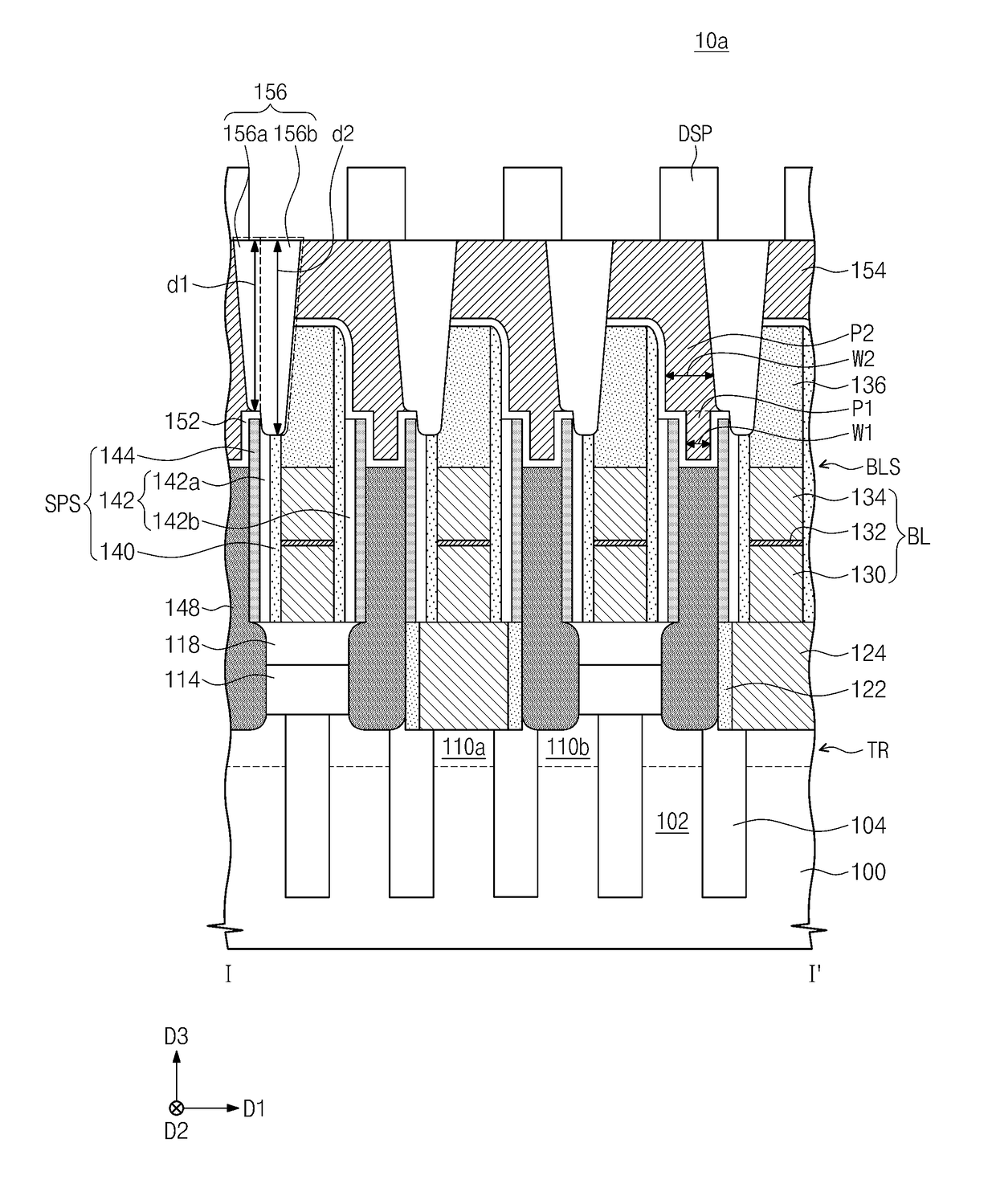
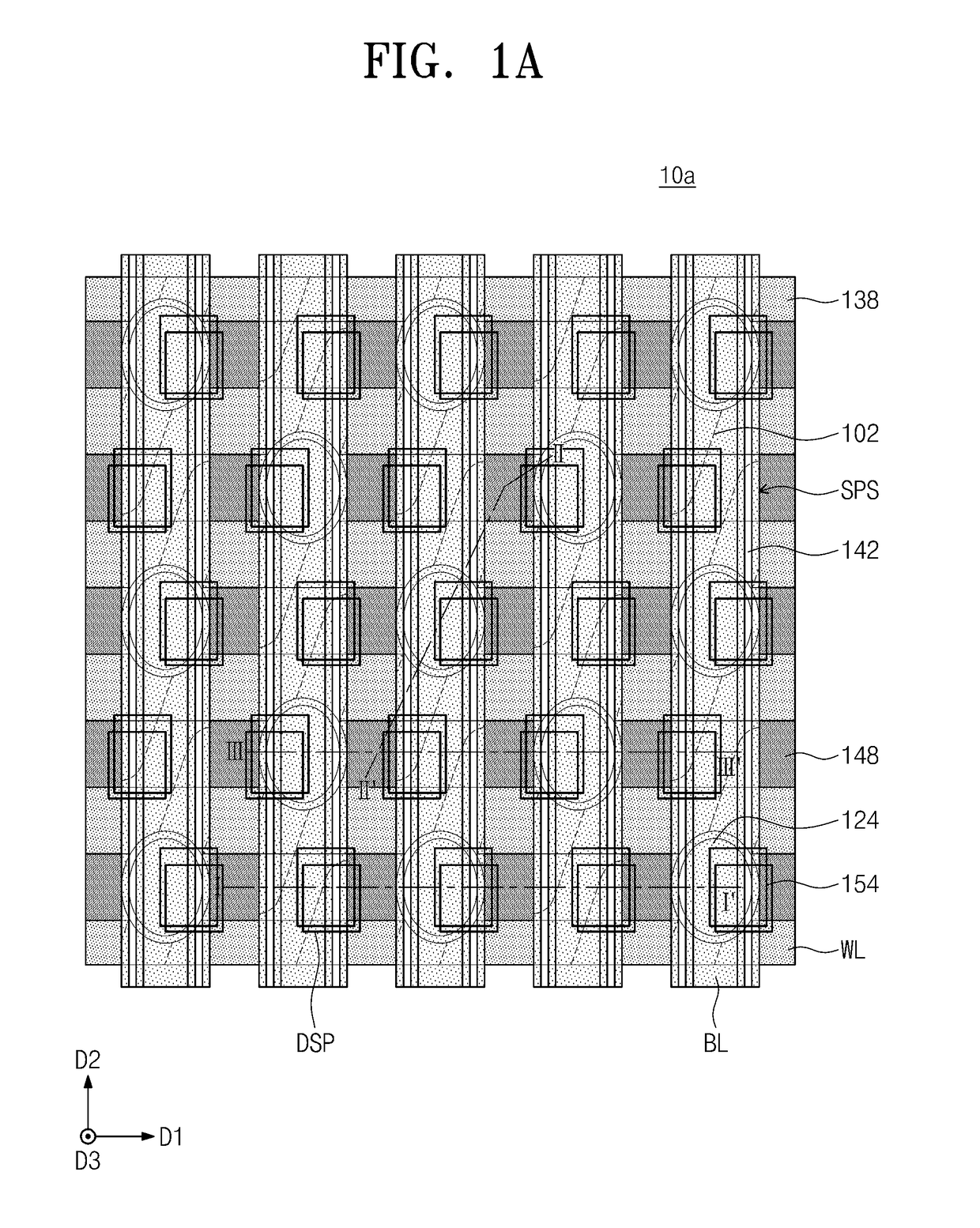
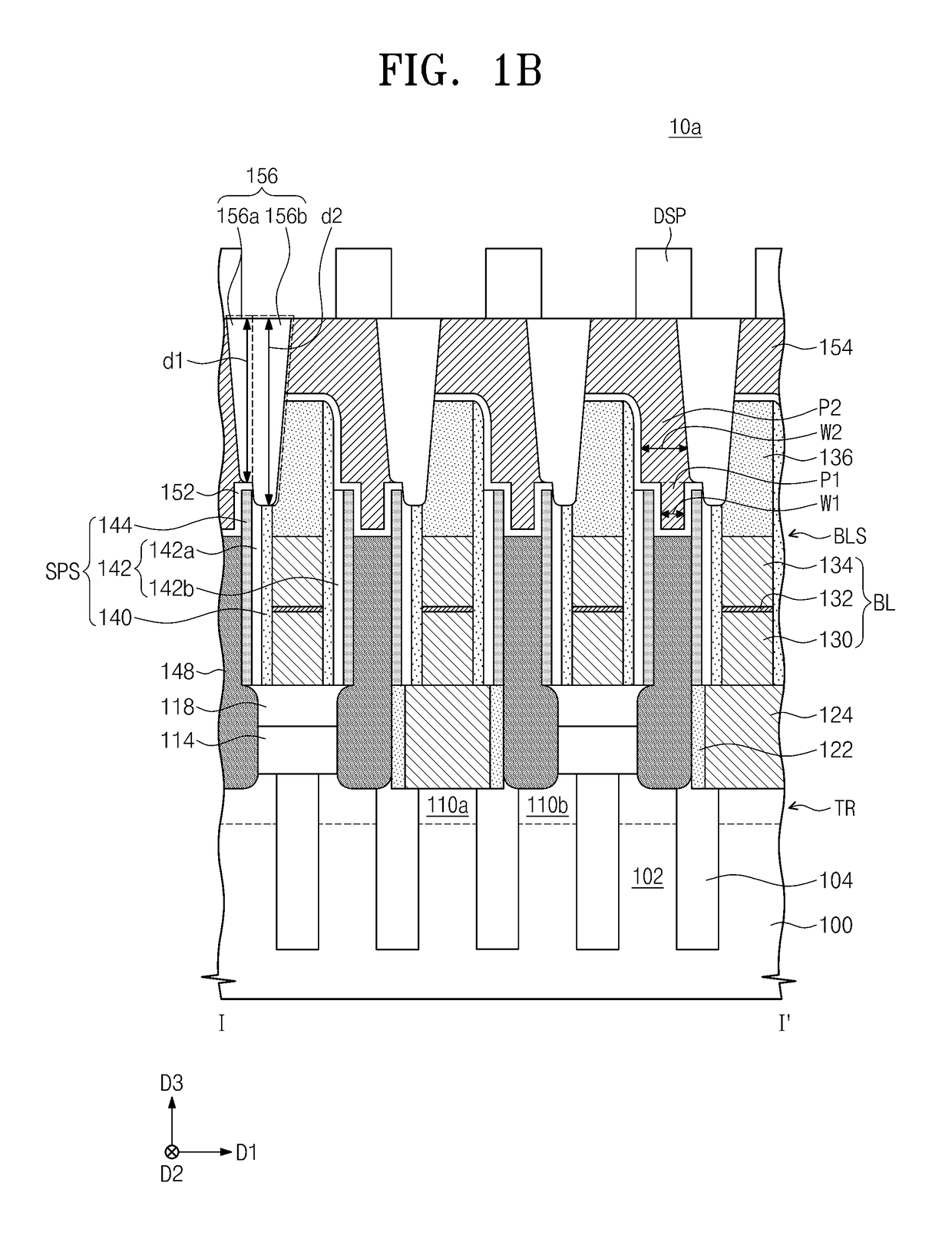
[0018]The present disclosure now will be described more fully hereinafter with reference to the accompanying drawings, in which various embodiments are shown. The invention may, however, be embodied in many different forms and should not be construed as limited to the example embodiments set forth herein. These example embodiments are just that—examples—and many implementations and variations are possible that do not require the details provided herein. It should also be emphasized that the disclosure provides details of alternative examples, but such listing of alternatives is not exhaustive. Furthermore, any consistency of detail between various examples should not be interpreted as requiring such detail—it is impracticable to list every possible variation for every feature described herein. The language of the claims should be referenced in determining the requirements of the invention.

[0019]It will be understood that, although the terms first, second, third etc. may be used here...


PUM


Abstract

According to some embodiments, a semiconductor device may include gate structures on a substrate; first and second impurity regions formed in the substrate and at both sides of each of the gate structures; conductive line structures provided to cross the gate structures and connected to the first impurity regions; and contact plugs connected to the second impurity regions, respectively. For each of the conductive line structures, the semiconductor device may include a first air spacer provided on a sidewall of the conductive line structure; a first material spacer provided between the conductive line structure and the first air spacer; and an insulating pattern provided on the air spacer. The insulating pattern may include a first portion and a second portion, and the second portion may have a depth greater than that of the first portion and defines a top surface of the air spacer.

Description

CROSS-REFERENCE TO RELATED APPLICATIONS[0001]This U.S. non-provisional patent application claims priority under 35 U.S.C. §119 to Korean Patent Application No. 10-2015-0154001, filed on Nov. 3, 2015, in the Korean Intellectual Property Office, the entire contents of which are hereby incorporated by reference.BACKGROUND OF THE INVENTION[0002]The present disclosure relates to semiconductor devices and methods of fabricating the same, and in particular, to semiconductor devices with an air spacer and methods of fabricating the same.[0003]Due to their small-sized, multifunctional, and / or low-cost characteristics, semiconductor devices are being esteemed as important elements in the electronic industry. The semiconductor devices may memory devices for storing data, logic devices for processing data, or hybrid devices including both of memory and logic elements.[0004]In general, a semiconductor device may include patterns vertically stacked on a substrate and contact plugs for electricall...

Claims


Application Information

Patent Timeline
Patent Type & Authority Applications(United States)
IPC IPC(8): H01L21/768H01L23/532H01L23/535
CPCH01L21/7682H01L23/535H01L21/76895H01L21/76805H01L21/76849H01L23/5329H10B12/315H10B12/34H10B12/053H10B12/0335
Inventor LEE, MYEONG-DONGKIM, KEUNNAMLEE, DONGRYULCHOI, MINSEONGCHOI, JIMINKIM, YONG KWANCHO, CHANGHYUNHWANG, YOOSANG
Owner SAMSUNG ELECTRONICS CO LTD
Why Eureka
Try Eureka