
Methods of fabricating package substrates having embedded circuit patterns

a technology of embedded circuit patterns and substrates, which is applied in the direction of lithographic masks, printed element electric connection formation, semiconductor/solid-state device details, etc., can solve the problem of difficulty in accurately or uniformly controlling the pitch size of the circuit pattern

Inactive Publication Date: 2017-02-23
SK HYNIX INC
View PDF2 Cites 2 Cited by
  • Summary
  • Abstract
  • Description
  • Claims
  • Application Information

AI Technical Summary

Benefits of technology

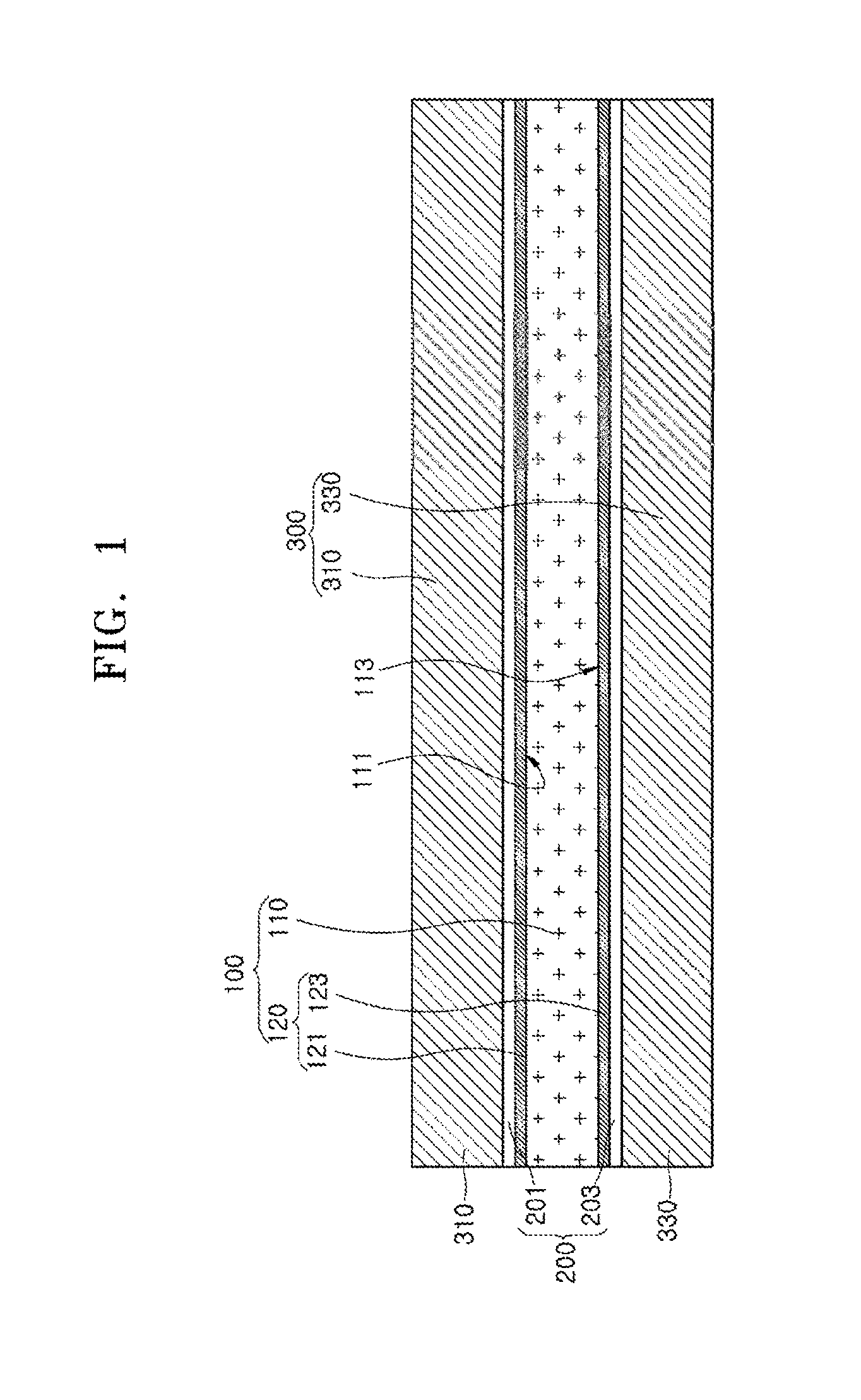
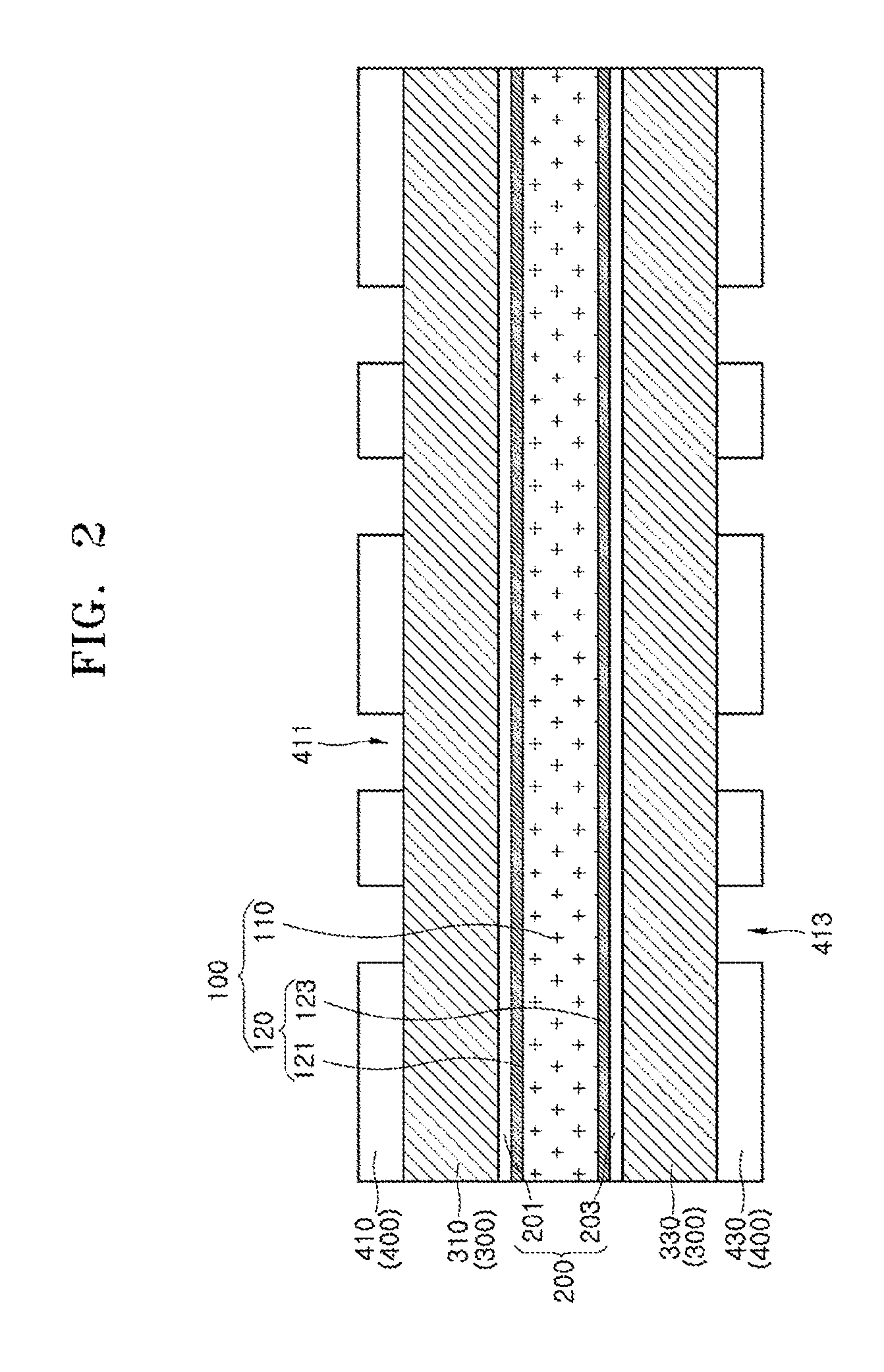
The present patent relates to semiconductor package technologies and, more particularly, to package substrates having embedded circuit patterns. The technical effects of the patent include providing methods for fabricating package substrates with fine circuit patterns having a uniform pitch size, as well as methods for forming isolation trenches and circuit patterns in the conductive layer of the substrate. The resulting package substrates can be used in electronic systems such as memory cards and semiconductor packages. The methods may include forming an isolation trench in the conductive layer, adding a first dielectric layer to provide an isolation wall portion filling the isolation trench, recessing the conductive layer to form circuit patterns, adding a second dielectric layer covering the circuit patterns, and patterning the first and second dielectric layers to expose portions of the circuit patterns.

Problems solved by technology

That is, it may be difficult to accurately or uniformly control a pitch size of the circuit patterns.

Method used


Image

  • Methods of fabricating package substrates having embedded circuit patterns
  • Methods of fabricating package substrates having embedded circuit patterns
  • Methods of fabricating package substrates having embedded circuit patterns

Examples


Embodiment Construction

[0012]Various embodiments may be directed to package substrates having embedded circuit patterns, methods of fabricating the same, semiconductor packages including the same, electronic systems including the same, and memory cards including the same.

[0013]According to an embodiment, there is provided a method of fabricating a package substrate. The method may include forming an isolation trench in a conductive layer, forming a first dielectric layer on the conductive layer to provide an isolation wall portion filling the isolation trench, recessing the conductive layer to form circuit patterns in circuit trenches defined and separated by the isolation wall portion, forming a second dielectric layer covering the circuit patterns, and patterning the first and second dielectric layers to expose portions of the circuit patterns. The exposed portions of the circuit patterns may act as connectors.

[0014]According to an embodiment, there is provided a method of fabricating a package substrat...


PUM


Abstract

There is provided a method of fabricating a package substrate. The method may include forming an isolation trench in a conductive layer, and forming a first dielectric layer on the conductive layer to provide an isolation wall portion filling the isolation trench. The method may include recessing the conductive layer to form circuit patterns in circuit trenches defined and separated by the isolation wall portion. The method may include forming a second dielectric layer covering the circuit patterns, and patterning the first and second dielectric layers to expose portions of the circuit patterns. The exposed portions of the circuit patterns may act as connectors.

Description

CROSS-REFERENCE TO RELATED APPLICATION[0001]The present application claims priority under 35 U.S.C 119(a) to Korean Patent Application No. 10-2015-0117456, filed on Aug. 20, 2015, in the Korean Intellectual Property Office, which is incorporated herein by reference in its entirety.BACKGROUND[0002]1. Technical Field[0003]Embodiments of the present disclosure generally relate to semiconductor package technologies and, more particularly, to package substrates having embedded circuit patterns, methods of fabricating the same, and semiconductor packages including the same.[0004]2. Related Art[0005]Semiconductor packages capable of processing a large amount of data are increasingly in demand with the development of smaller electronic systems such as mobile systems. As a result, package substrates including circuit patterns having a fine pitch size have been required. Electronic devices, for example, semiconductor chips may be mounted on the package substrates. Package substrates may inclu...

Claims


Application Information

Patent Timeline
Patent Type & Authority Applications(United States)
IPC IPC(8): H01L21/48H05K3/46H05K3/06
CPCH01L21/4857H05K2203/0548H05K3/4697H05K3/06H01L23/12H01L23/48H01L24/26H01L24/27H01L24/31H05K3/40H01L2224/331H01L2224/3301H01L23/49816H01L23/49827H05K1/181H05K3/007H05K3/4007H05K2203/0369H05K2203/041H05K2203/049H01L2924/181H01L2224/16H01L2224/48228H01L2924/15311H01L21/6835H01L2221/68345H01L2221/68386H01L2924/00012
Inventor KIM, MYEONG SEOBKIM, JAE YOUNGMOON, KI ILL
Owner SK HYNIX INC
Learn More