
Electronic device with multi-band antenna for supporting carrier aggregation using non-segmented conductive border member

a technology of conductive border member and electronic device, which is applied in the direction of antenna earthing, elongated active element feed, resonance antenna, etc., can solve the problems of low yield upon metal processing, spoiling appearance, and the technique of designing a receiver antenna

Active Publication Date: 2017-02-02
SAMSUNG ELECTRO MECHANICS CO LTD
View PDF2 Cites 18 Cited by
  • Summary
  • Abstract
  • Description
  • Claims
  • Application Information

AI Technical Summary

Benefits of technology

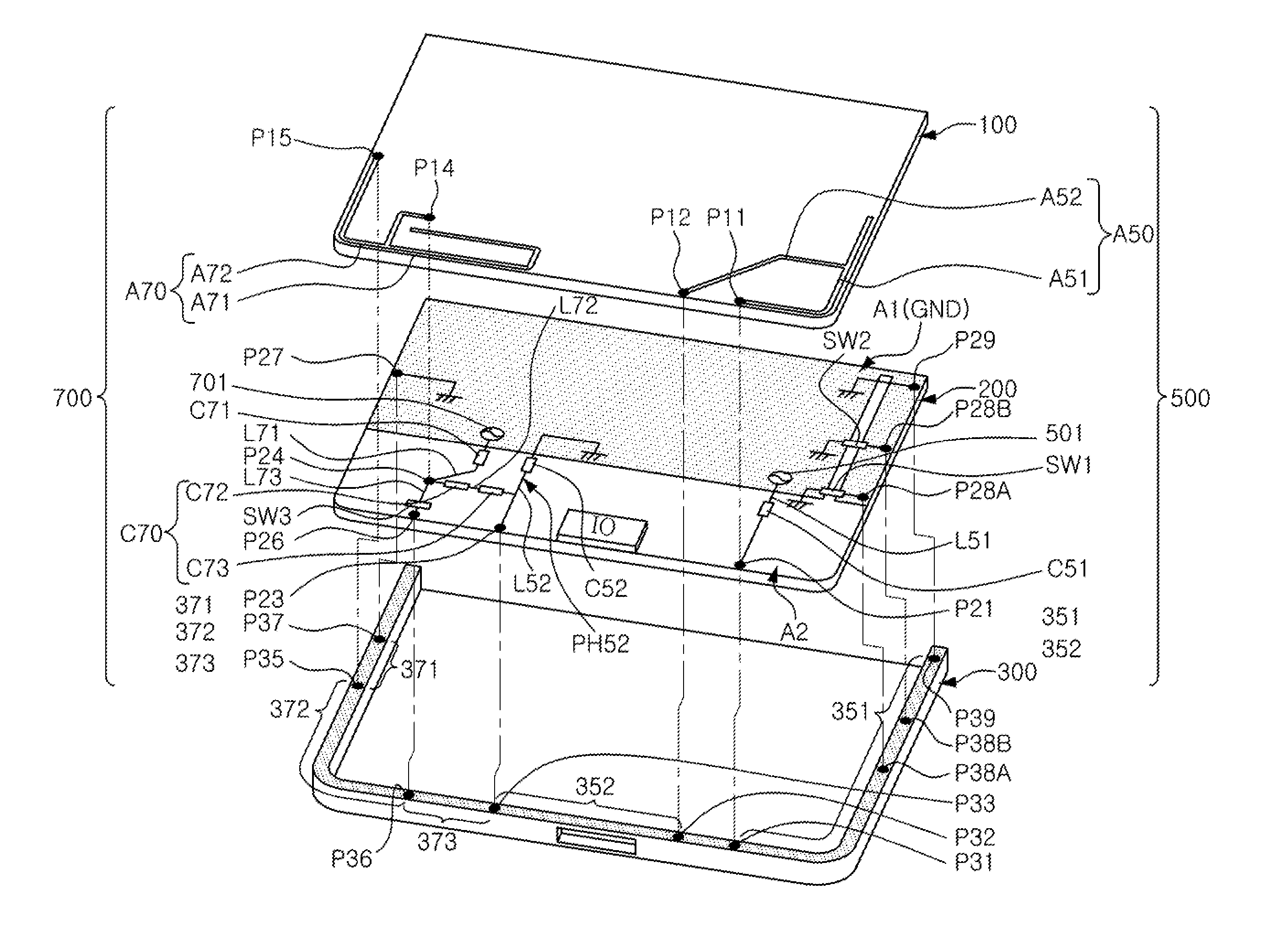
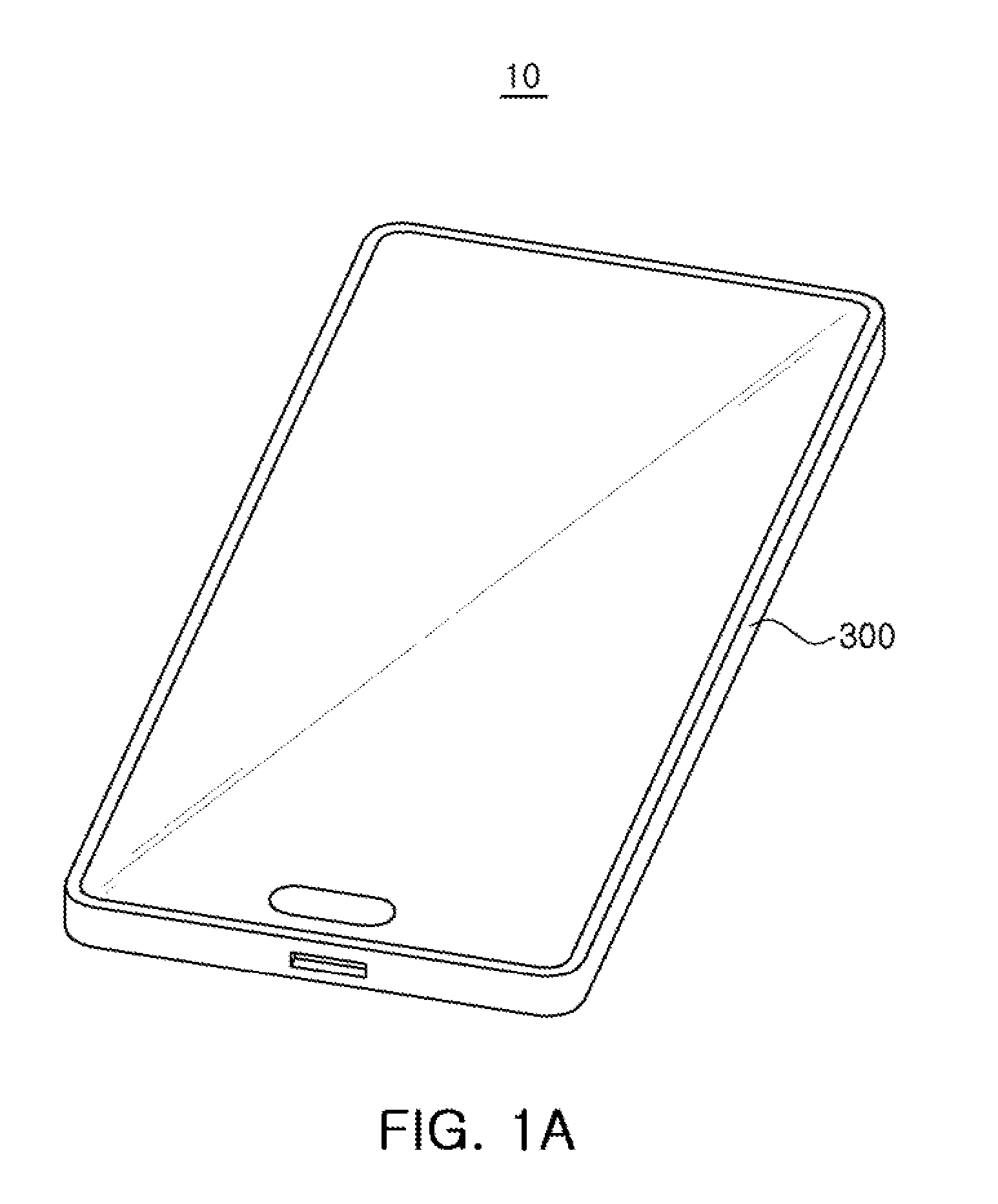
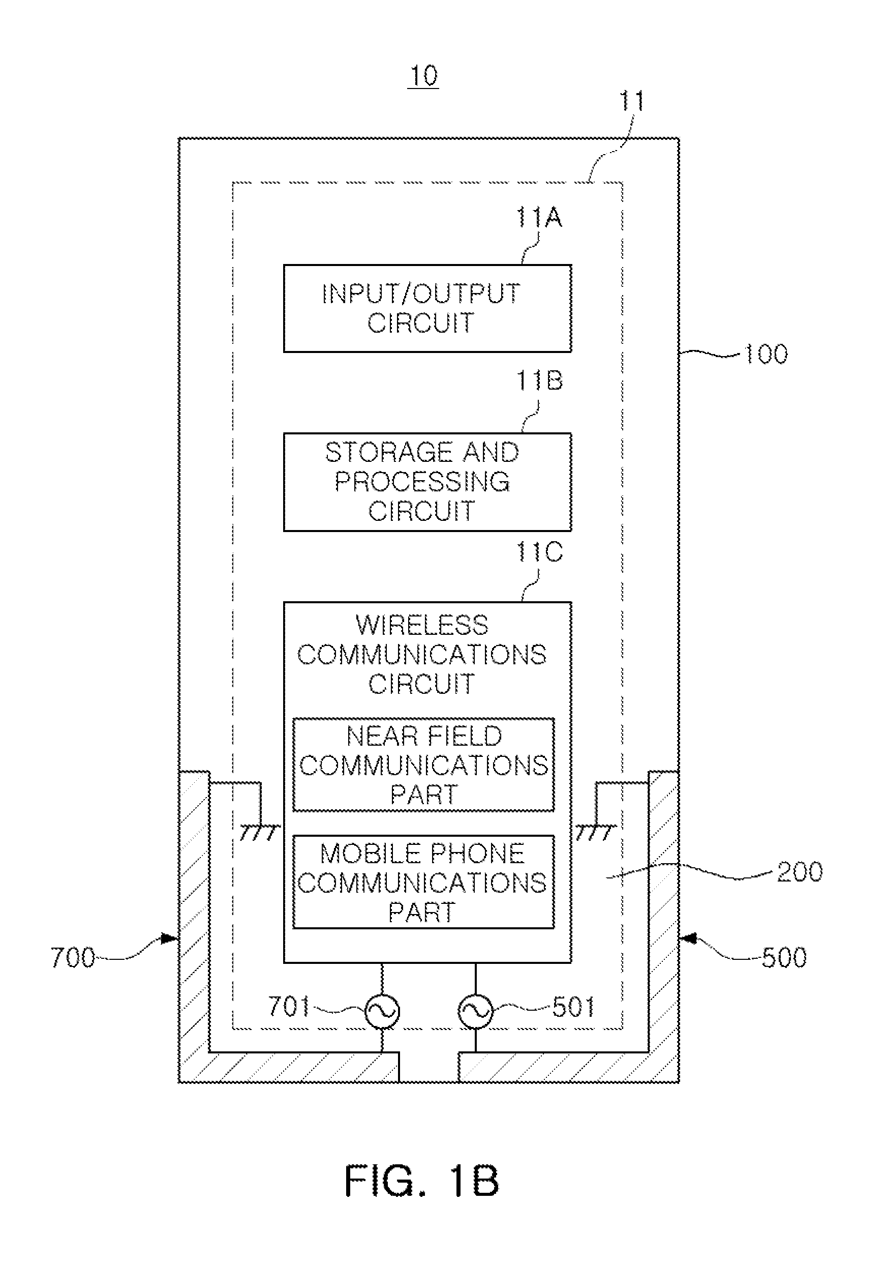
The patent describes an electronic device with two antennas that form multiple resonances for covering different multi-bands. The first antenna is connected to the first feed terminal and the conductive border member, while the second antenna is connected to the second feed terminal and the conductive border member. A bypass conductor is used to prevent interference between the two antennas. The first antenna has a first electrical length and a first bridge antenna pattern, while the second antenna has a second electrical length and a second bridge antenna pattern. The first and second antennas can be designed to cover different multi-bands without overlapping. The technical effect of this design is improved wireless communication capabilities of the electronic device.

Problems solved by technology

However, segmenting of the conductive border member may spoil an appearance and have a low yield upon metal processing.
To this end, a technique of designing a receiver antenna has been highlighted as an important problem.
Further, due to the structure of the electronic device using the conductive border member, the number of receiver antennas may be increased and, therefore, an isolation problem between the antennas may occur.

Method used


Image

  • Electronic device with multi-band antenna for supporting carrier aggregation using non-segmented conductive border member
  • Electronic device with multi-band antenna for supporting carrier aggregation using non-segmented conductive border member
  • Electronic device with multi-band antenna for supporting carrier aggregation using non-segmented conductive border member

Examples


Embodiment Construction

[0055]The following detailed description is provided to assist the reader in gaining a comprehensive understanding of the methods, apparatuses, and / or systems described herein. However, various changes, modifications, and equivalents of the systems, apparatuses and / or methods described herein will be apparent to one of ordinary skill in the art. The progression of processing steps and / or operations described is an example; however, the sequence of and / or operations is not limited to that set forth herein and may be changed as is known in the art, with the exception of steps and / or operations necessarily occurring in a certain order. Also, descriptions of functions and constructions that are well known to one of ordinary skill in the art may be omitted for increased clarity and conciseness.

[0056]The features described herein may be embodied in different forms, and are not to be construed as being limited to the examples described herein. Rather, the examples described herein have bee...


PUM


Abstract

An electronic device including a multi-band antenna, a cover, a substrate, and a conductive border member is disclosed, where the device includes a first feed terminal connected to a circuit of a substrate embedded in the device, a second feed terminal connected to the circuit and insulated from the first feed terminal, a ground disposed on the substrate, a conductive border member continuously disposed along a periphery of the electronic device, a first antenna connected to the first feed terminal and the conductive border member, and the first antenna forming a multiple resonance for covering a first multi-band having a plurality of bands, a second antenna connected to the second feed terminal and the conductive border member and the second antenna forming a multiple resonance for covering a second multi-band, and a bypass conductor to bypass interference signals generated by the first antenna and the second antenna to the ground.

Description

CROSS-REFERENCE TO RELATED APPLICATION[0001]This application claims the benefit under 35 U.S.C. §119(a) of Korean Patent Application Nos. 10-2015-0108246 filed on Jul. 30, 2015 and 10-2015-0189250 filed on Dec. 30, 2015 in the Korean Intellectual Property Office, the entire disclosure of which is incorporated herein by reference for all purposes.BACKGROUND[0002]1. Field[0003]The following description relates to an electronic device including a multi-band antenna that supports carrier aggregation (CA) using a non-segmented conductive border member.[0004]2. Description of Related Art[0005]Portable electronic devices, such as smartphones, being designed to include a metal exterior have become popular. The metal exterior has drawn much attention to improve external rigidity and to protect an interior of the portable electronic device.[0006]For example, a conductive border member is used in the exterior design of the electronic device, and a conductor frame is embedded in the interior of...

Claims


Application Information

Patent Timeline
Patent Type & Authority Applications(United States)
IPC IPC(8): H01Q1/24H03H7/38H01Q1/52H01Q9/04H01Q5/50H01Q1/48
CPCH01Q1/243H01Q5/50H03H7/38H01Q1/523H01Q9/04H01Q1/48H01Q5/20H01Q1/242H01Q1/50H01Q1/521H01Q9/42H01Q5/328H01Q5/335
Inventor KIM, NAM KIJEON, DAE SEONGCHEON, YOUNG MINPARK, HYUN DOLIM, DAE KI
Owner SAMSUNG ELECTRO MECHANICS CO LTD
Learn More