Light-Emitting Element, Display Device, Electronic Device, and Lighting Device

a technology of light-emitting elements and electronic devices, which is applied in the direction of organic semiconductor devices, organic chemistry, indium organic compounds, etc., can solve the problems of poor electron-accepting properties, difficult excitation through direct recombination of carriers or efficient light emission by light-emitting elements in some cases, and achieve high emission efficiency, reduce power consumption, and high reliability

Pending Publication Date: 2017-01-26
SEMICON ENERGY LAB CO LTD
View PDF2 Cites 161 Cited by
  • Summary
  • Abstract
  • Description
  • Claims
  • Application Information

AI Technical Summary

Benefits of technology

[0026]With one embodiment of the present invention, a light-emitting element that contains a phosphorescent material and has high emission efficiency can be provided. With one embodiment of the present invention, a light-emitting element with reduced power consumption can be provided. With one embodiment of the present invention, a light-emitting element with high reliability can be provided. With one embodiment of the present invention, a novel light-emitting element can be provided. With one embodiment of the present invention, a novel light-emitting device can be provided. With one embodiment of the present invention, a novel display device can be provided.

Problems solved by technology

Although the pyridine skeleton and the nitrogen-containing five-membered heterocyclic skeleton have high triplet excitation energy, they have poor electron-accepting property.
As a result, when an iridium complex with a high light emission energy is used, excitation through direct recombination of carriers or efficient light emission by a light-emitting element is difficult in some cases.

Method used


Image

  • Light-Emitting Element, Display Device, Electronic Device, and Lighting Device
  • Light-Emitting Element, Display Device, Electronic Device, and Lighting Device
  • Light-Emitting Element, Display Device, Electronic Device, and Lighting Device

Examples


embodiment 1

[0131]In this embodiment, a light-emitting element of one embodiment of the present invention will be described below with reference to FIGS. 1A and 1B and FIGS. 2A and 2B.

[0132]First, a structure of the light-emitting element of one embodiment of the present invention will be described with reference to FIGS. 1A and 1B.

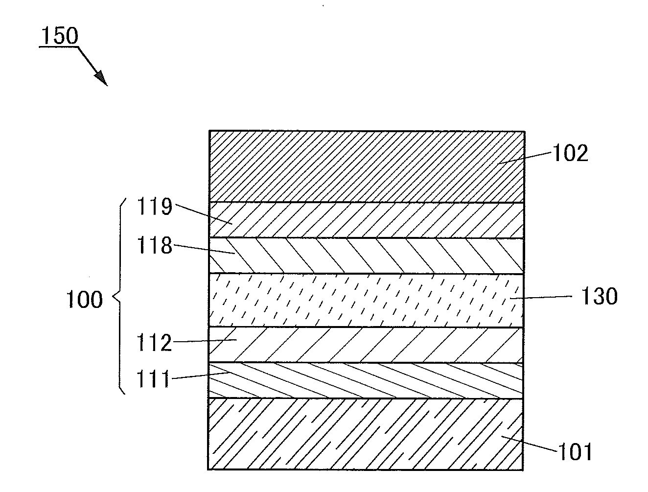
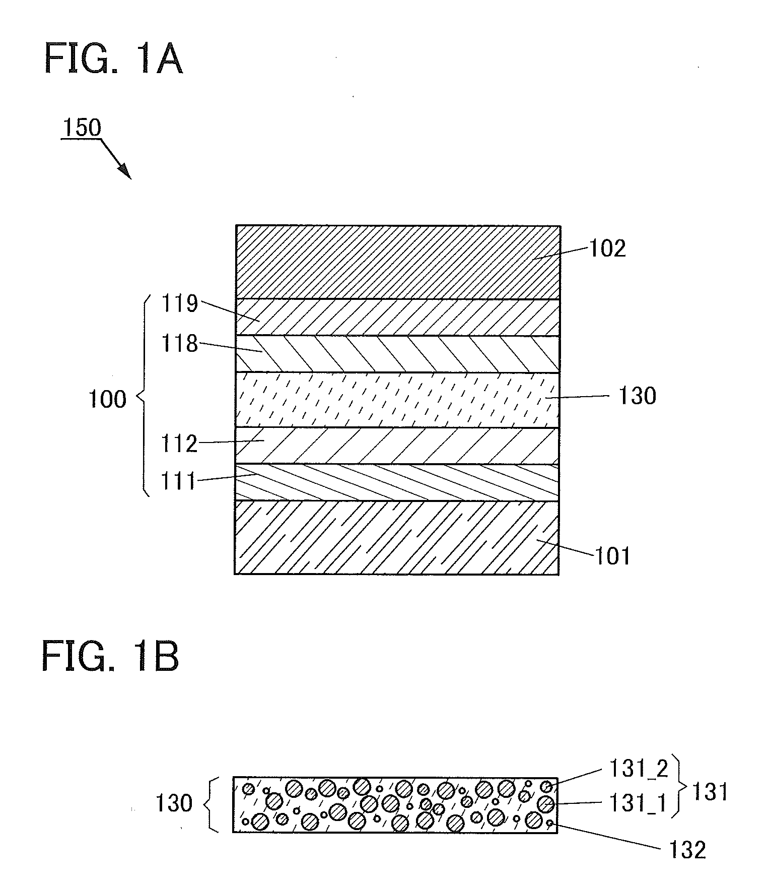
[0133]FIG. 1A is a schematic cross-sectional view of a light-emitting element 150 of one embodiment of the present invention.

[0134]The light-emitting element 150 includes a pair of electrodes (an electrode 101 and an electrode 102) and an EL layer 100 between the pair of electrodes. The EL layer 100 includes at least a light-emitting layer 130.

[0135]The EL layer 100 illustrated in FIG. 1A includes functional layers such as a hole-injection layer 111, a hole-transport layer 112, an electron-transport layer 118, and an electron-injection layer 119, in addition to the light-emitting layer 130.

[0136]In this embodiment, although description is given assuming that the elec...

embodiment 2

[0311]In this embodiment, light-emitting elements each having a structure different from that described in Embodiment 1 are described below with reference to FIGS. 3A to 3C and FIGS. 4A to 4C. In FIGS. 3A to 3C and FIGS. 4A to 4C, a portion having a function similar to that in FIG. 1A is represented by the same hatch pattern as in FIG. 1A and not especially denoted by a reference numeral in some cases. In addition, common reference numerals are used for portions having similar functions, and a detailed description of the portions is omitted in some cases.

[0312]FIG. 3A is a schematic cross-sectional view of a light-emitting element 250.

[0313]The light-emitting element 250 illustrated in FIG. 3A includes a plurality of light-emitting units (a light-emitting unit 106 and a light-emitting unit 108 in FIG. 3A) between a pair of electrodes (the electrode 101 and the electrode 102). One of light-emitting units preferably has the same structure as the EL layer 100 illustrated in FIGS. 1A an...

embodiment 3

[0395]In this embodiment, examples of light-emitting elements having structures different from those described in Embodiments 1 and 2 are described below with reference to FIGS. 5A and 5B, FIGS. 6A and 6B, FIGS. 7A to 7C, and FIGS. 8A to 8C.

[0396]FIGS. 5A and 5B are cross-sectional views each illustrating a light-emitting element of one embodiment of the present invention. In FIGS. 5A and 5B, a portion having a function similar to that in FIG. 1A is represented by the same hatch pattern as in FIG. 1A and not especially denoted by a reference numeral in some cases. In addition, common reference numerals are used for portions having similar functions, and a detailed description of the portions is omitted in some cases.

[0397]Light-emitting elements 260a and 260b in FIGS. 5A and 5B may have a bottom-emission structure in which light is extracted through the substrate 200 or may have a top-emission structure in which light emitted from the light-emitting element is extracted in the direc...


PUM

PropertyMeasurementUnit
transition energyaaaaaaaaaa
light emission energyaaaaaaaaaa
temperatureaaaaaaaaaa

Abstract

A light-emitting element with high emission efficiency. The light-emitting element includes a first organic compound, a second organic compound, and a guest material. The LUMO level of the first organic compound is lower than the LUMO level of the second organic compound. The HOMO level of the first organic compound is lower than the HOMO level of the second organic compound. The HOMO level of the guest material is higher than the HOMO level of the second organic compound. The energy difference between the LUMO level of the guest material and the HOMO level of the guest material is larger than the energy difference between the LUMO level of the first organic compound and the HOMO level of the second organic compound. The guest material has a function of converting triplet excitation energy into light emission. The first organic compound and the second organic compound form an exciplex.

Description

TECHNICAL FIELD[0001]One embodiment of the present invention relates to a light-emitting element, or a display device, an electronic device, and a lighting device each including the light-emitting element.[0002]Note that one embodiment of the present invention is not limited to the above technical field. The technical field of one embodiment of the invention disclosed in this specification and the like relates to an object, a method, or a manufacturing method. In addition, one embodiment of the present invention relates to a process, a machine, manufacture, or a composition of matter. Specifically, examples of the technical field of one embodiment of the present invention disclosed in this specification include a semiconductor device, a display device, a liquid crystal display device, a light-emitting device, a lighting device, a power storage device, a memory device, a method for driving any of them, and a method for manufacturing any of them.BACKGROUND ART[0003]In recent years, re...

Claims


Application Information

Patent Timeline
Patent Type & Authority Applications(United States)
IPC IPC(8): H01L51/50C07F15/00C09K11/06H01L27/32
CPCH01L51/5028C09K2211/185H01L51/5016H01L51/5072H01L51/5056H01L27/322H01L27/3244H01L27/323C07F15/0033C09K11/06H01L2251/552H01L51/0085H01L51/0074H01L51/0072H01L51/0067H01L51/006H01L51/0061H01L51/0052H01L51/0071C09K2211/1007C09K2211/1059H01L51/5004H10K50/11H10K2101/40H10K50/12C09K2211/1011H10K85/633H10K85/6576H10K85/6572H10K85/657H10K85/342H10K50/121H10K2101/10H10K2101/80H10K2101/90H10K2101/30H10K59/38H10K59/1213H10K59/87H10K50/84H10K85/654H10K2101/25H10K50/15H10K50/16H10K59/12H10K59/40H10K85/615H10K85/636
Inventor SEO, SATOSHITAKAHASHI, TATSUYOSHIWATABE, TAKEYOSHIMITSUMORI, SATOMI
Owner SEMICON ENERGY LAB CO LTD
Why Eureka
Try Eureka