Power semiconductor device

a technology of semiconductor devices and semiconductors, applied in the direction of semiconductor devices, basic electric elements, electrical equipment, etc., can solve the problem of inability to reduce turn-on losses, and achieve the effect of reducing turn-on losses, increasing the time rate of change in collector voltage, and enhancing the modulation effect of conductivity to the contribution of collector curren

Active Publication Date: 2016-12-22
MITSUBISHI ELECTRIC CORP
View PDF7 Cites 12 Cited by
  • Summary
  • Abstract
  • Description
  • Claims
  • Application Information

AI Technical Summary

Benefits of technology

[0007]It is therefore an object of the present invention to provide a power semiconductor device capable of reducing the turn-on loss in addition to reductions in the conduction loss and the turn-off loss even under the certain condition of the time rate of change in collector voltage.
[0016]According to the present invention, while ON / OFF of a collector current is controlled with a gate potential applied to an active trench gate (6a), a conductivity modulation effect contributive to the collector current can be enhanced by disposing isolated dummy trench gates (6b) fixed to an emitter potential with the active trench gate (6a) interposed therebetween. Additionally, by disposing active dummy trench gates (6c) fixed to the gate potential such that these trench gates are interposed therebetween, a time rate of change in collector voltage can be made more gradual by a parasitic capacitance between a gate electrode and a collector electrode, and a turn-on loss can be reduced under a certain condition of the time rate of change in collector voltage.

Problems solved by technology

A switching loss is made up of two components, which are a turn-on loss when the IGBT is switched from OFF to ON and a turn-off loss when the IGBT is switched from ON to OFF, and the IGBT having a higher density of trench gates and the increased number of dummy trench gates has a problem that although the conduction loss and the turn-off loss can be reduced, the turn-on loss cannot be reduced under a certain condition of a time rate of change in collector voltage.

Method used


Image

  • Power semiconductor device
  • Power semiconductor device
  • Power semiconductor device

Examples


first embodiment

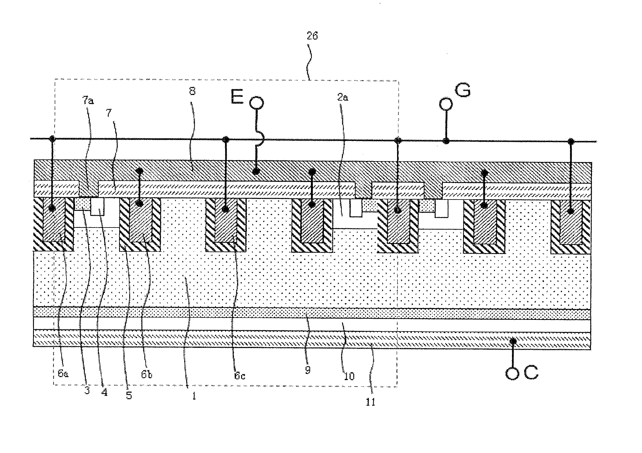
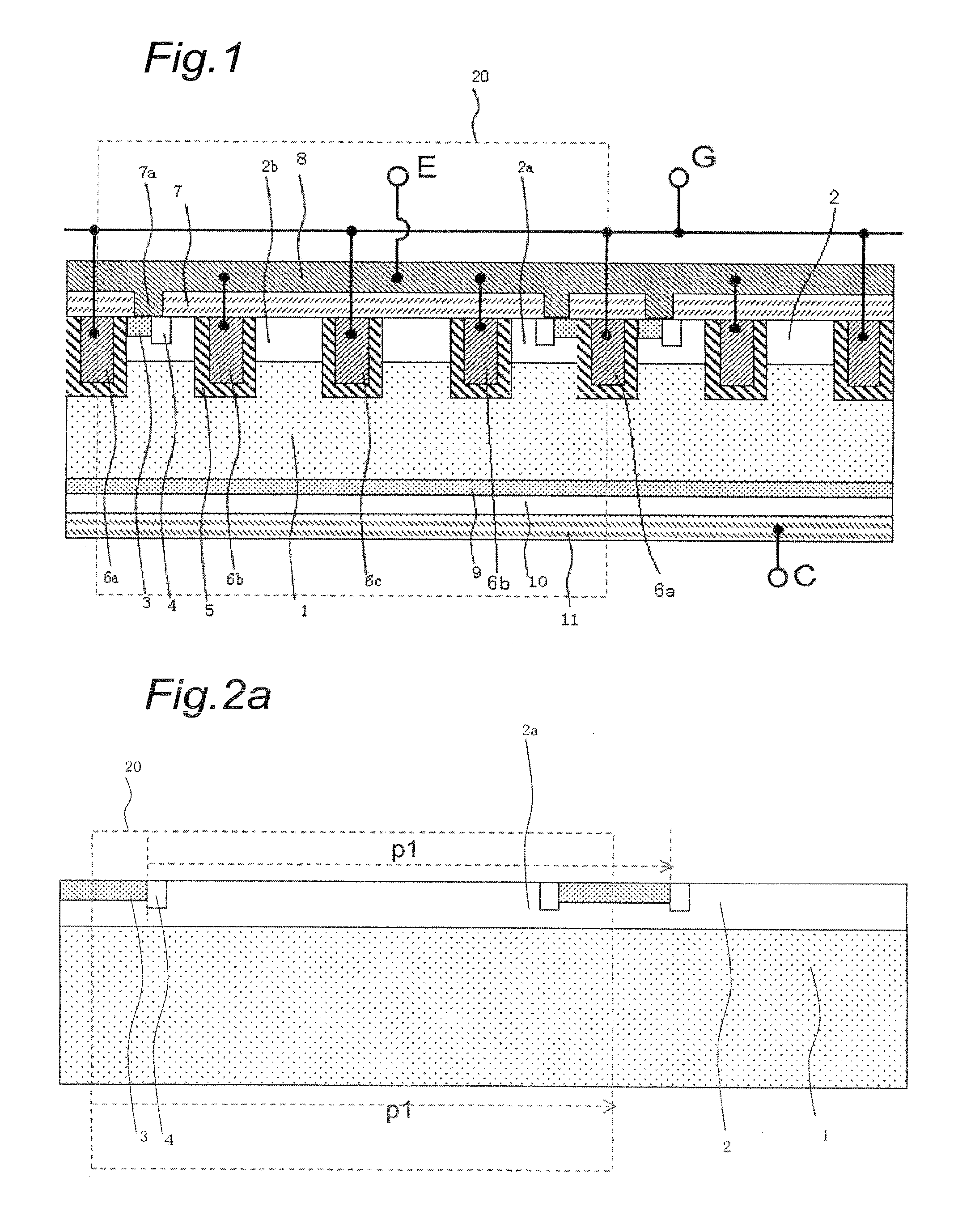
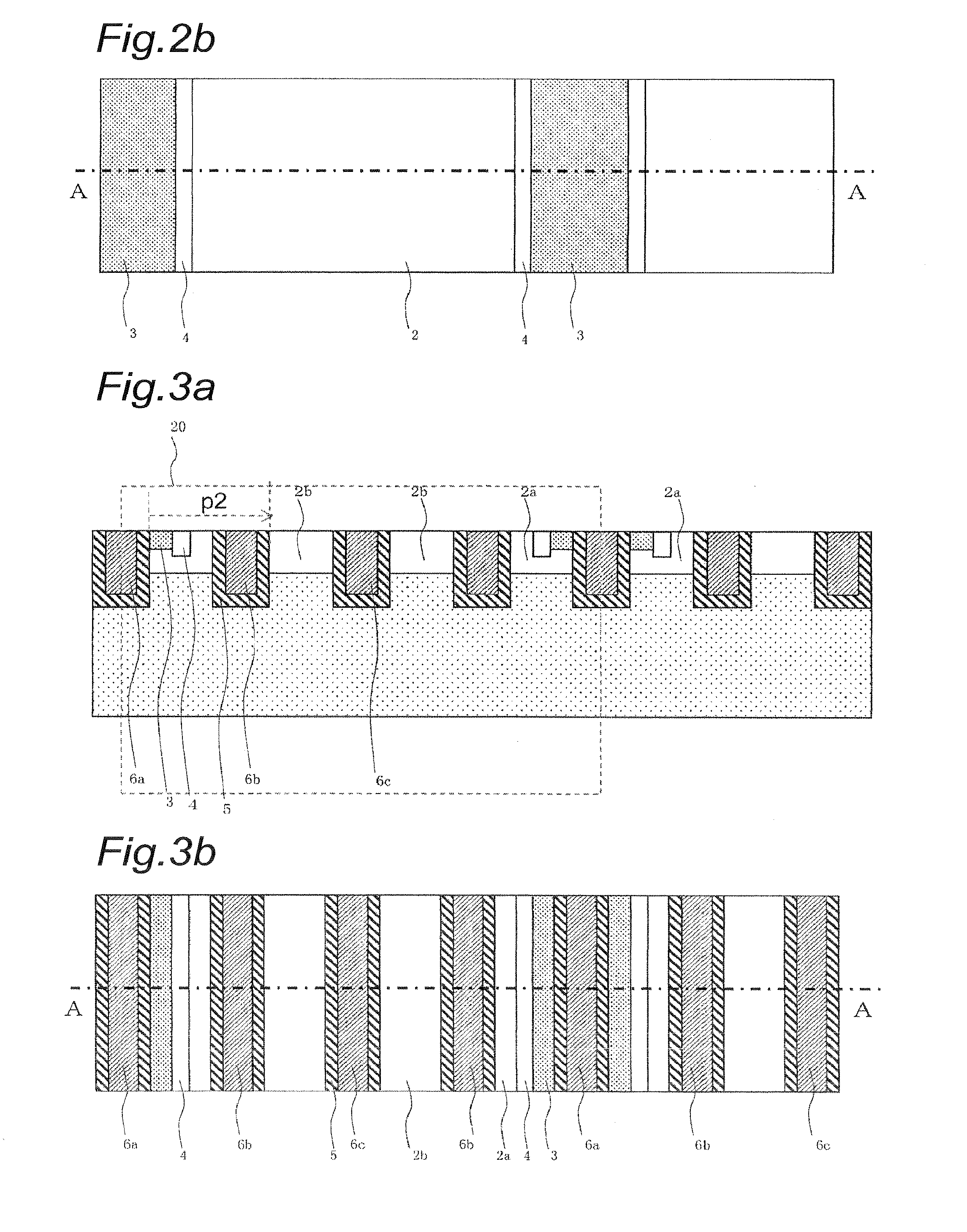
[0037]FIG. 1 is a cross-sectional view of a vertical trench IGBT according to a first embodiment of the present invention generally denoted by 20 and a portion surrounded by a dashed line is a unit IGBT. The trench IGBT 20 includes an n-type (first-conductive-type) base region 1 (a first-conductive-type first base region) having a first principal surface (front surface) and a second principal surface (back surface) opposite to the first principal surface. The front surface of the n-type base region 1 on the first principal surface side includes a selectively formed p-type (second-conductive-type) base region 2.

[0038]The trench IGBT 20 includes n-type emitter regions 3 (first-conductive-type emitter regions) selectively formed shallower than the p-type base region 2 in a stripe shape in the front surface of the p-type base region 2 on the first principal surface side and p-type contact regions 4 (second-conductive-type first contact regions) formed shallower than the p-type base regi...

second embodiment

[0074]FIG. 12 is a cross-sectional view of a trench IGBT according to a second embodiment of the present invention generally denoted by 23 and a portion surrounded by a dashed line is a unit IGBT. In FIG. 12, the same reference numerals as FIG. 1 denote the same or corresponding portions.

[0075]The trench IGBT 23 according to the second embodiment of the present invention has a structure having the p-type contact region 4 disposed in the p-type base region 2b interposed between the two active dummy trench gates 6c in the trench IGBT 22a (see FIG. 7) according to the modification example of the first embodiment. An opening region 7c is formed in the interlayer insulating film 7 such that the p-type contact region 4 is partially exposed, and the p-type contact region 4 is connected to the emitter electrode 8.

[0076]Since only the p-type base region 2b interposed between the two active dummy trench gates 6c is provided with the p-type contact region 4 as described above, although a porti...

third embodiment

[0078]FIG. 13 is a cross-sectional view of a trench IGBT according to a third embodiment of the present invention generally denoted by 24 and a portion surrounded by a dashed line is a unit IGBT. In FIG. 13, the same reference numerals as FIG. 1 denote the same or corresponding portions.

[0079]The trench IGBT 24 according to the third embodiment of the present invention has a structure having a distance between the isolated dummy trench gate 6b and the active dummy trench gate 6c made narrower as compared to a distance between the active trench gate 6a and the isolated dummy trench gate 6b in the trench IGBT 20 (see FIG. 1) according to the first embodiment. Therefore, since it is not necessary to dispose a contact region in the p-type base region between the isolated dummy trench 6b and the active dummy trench gate 6c, the distance between the isolated dummy trench gate 6b and the active dummy trench gate 6c can be reduced to a minimum design rule of a semiconductor process.

[0080]In...


PUM


Abstract

In the present application, a power semiconductor device includes a first-conductive-type first base region having a first principal surface and a second principal surface opposite to the first principal surface, a second-conductive-type second base region disposed on the first principal surface and at least three groove parts parallel to each other disposed from a surface of the second base region. The device further includes insulating films covering inner walls of the respective groove parts, conductive trench gates filled on the insulating films, a first-conductive-type emitter region disposed in the second base region, and a second-conductive-type collector region disposed on the second principal surface of the first base region. The trench gates embedded in the first groove part and the third groove part are electrically connected to the gate electrode, and the trench gate embedded in the second groove part is electrically connected to the emitter electrode.

Description

FIELD OF THE INVENTION[0001]The present invention relates to a power semiconductor device and, more particularly, to a semiconductor device with trench gates such as an IGBT (Insulated Gate Bipolar Transistor).BACKGROUND OF THE INVENTION[0002]A conduction loss of a power semiconductor device such as an IGBT can be reduced by increasing a density of trench gates formed in a stripe shape on a semiconductor substrate front surface. For example, an IGBT with trench gates (hereinafter referred to as a “trench IGBT”) has an n-type emitter region, a p-type contact region, a p-type base region, an n-type base region, an n-type buffer region, and a p-type collector region formed in order on a semiconductor substrate from a surface toward a back surface thereof. Trench gates are formed into a stripe shape in the substrate front surface and are formed to penetrate the n-type emitter region and the p-type base region adjacently to the n-type emitter region and to reach the n-type base region. T...

Claims


Application Information

Patent Timeline
Patent Type & Authority Applications(United States)
IPC IPC(8): H01L29/739H01L29/08H01L29/10H01L29/66
CPCH01L29/7397H01L29/66348H01L29/1004H01L29/0821H01L29/1095H01L29/0804H01L29/407H01L29/0619H01L29/0696H01L29/78H01L29/739H01L21/28H01L29/4236H01L29/42356
Inventor FURUKAWA, AKIHIKOORITA, SHOICHIMURAOKA, HIROKINARAZAKI, ATSUSHIKAWAKAMI, TSUYOSHIMURAKAMI, YUJI
Owner MITSUBISHI ELECTRIC CORP
Why Eureka
Try Eureka