
Systems and methods for controlling aliasing in images captured by an array camera for use in super resolution processing using pixel apertures

a technology of array cameras and aliasing, applied in the field of super resolution processing, can solve the problems of affecting the overall form factor of the mobile device, image sensors are subject to various performance constraints,

Active Publication Date: 2016-10-27
PELICAN IMAGING CORP +1
View PDF8 Cites 91 Cited by
  • Summary
  • Abstract
  • Description
  • Claims
  • Application Information

AI Technical Summary

Benefits of technology

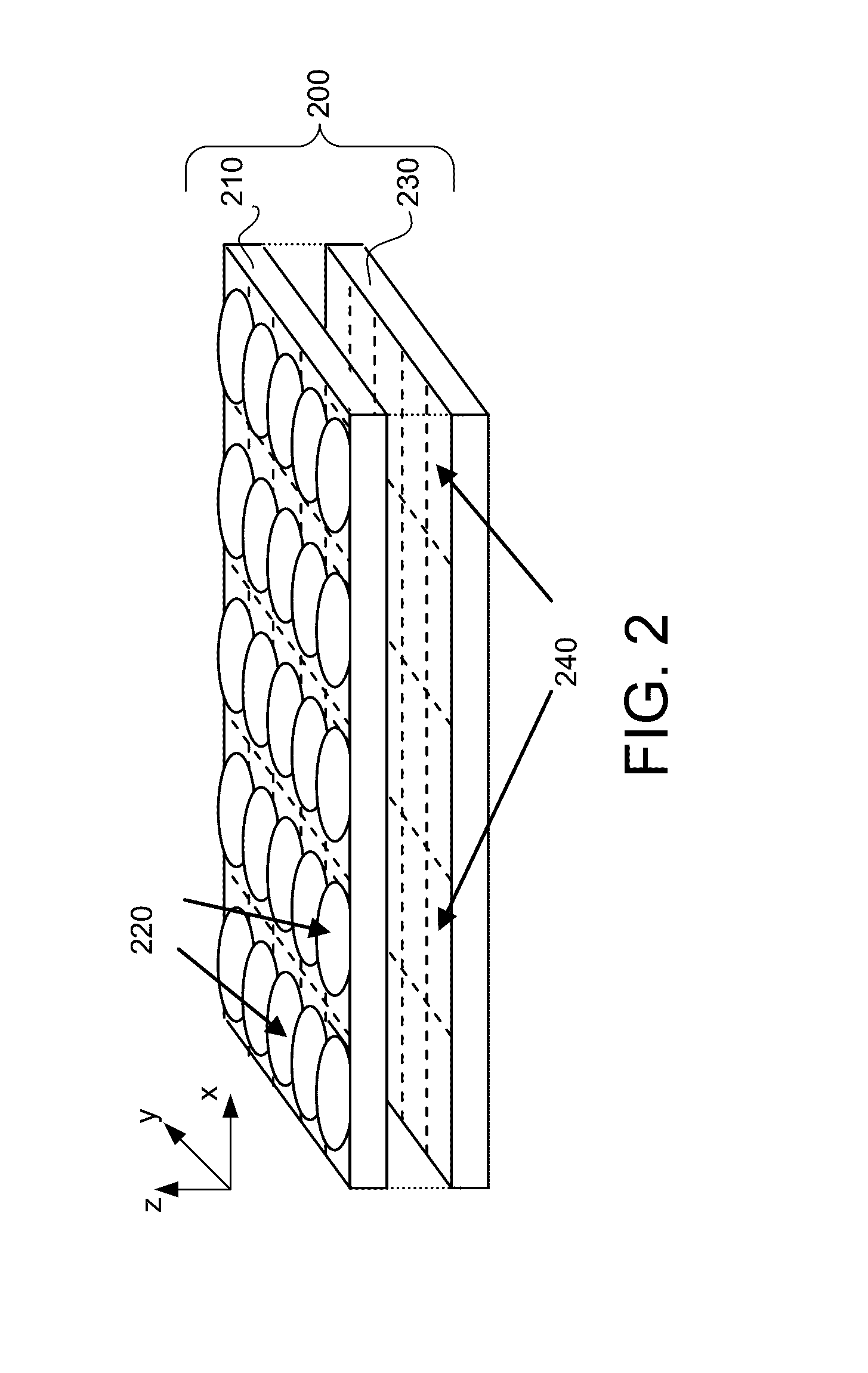
The patent text describes a method to prevent light from entering certain parts of a camera sensor. This is done by using a light blocking material to fill the gaps between the microlenses, which helps to block the light from entering the pixel stacks. The technical effect of this method is improved image quality and reduced noise in the camera sensor.

Problems solved by technology

Image sensors are subject to various performance constraints including, among others, dynamic range, signal to noise (SNR) ratio and low light sensitivity.
A challenge associated with increasing the number of pixels in an image sensor is that the lens system is dimensioned to span the image sensor.
The problem is most acute with mobile cameras, such as those used in mobile phones and consumer electronics devices, where the form factor of the lens system can significantly impact the overall form factor of the mobile device.

Method used


Image

  • Systems and methods for controlling aliasing in images captured by an array camera for use in super resolution processing using pixel apertures
  • Systems and methods for controlling aliasing in images captured by an array camera for use in super resolution processing using pixel apertures
  • Systems and methods for controlling aliasing in images captured by an array camera for use in super resolution processing using pixel apertures

Examples


Embodiment Construction

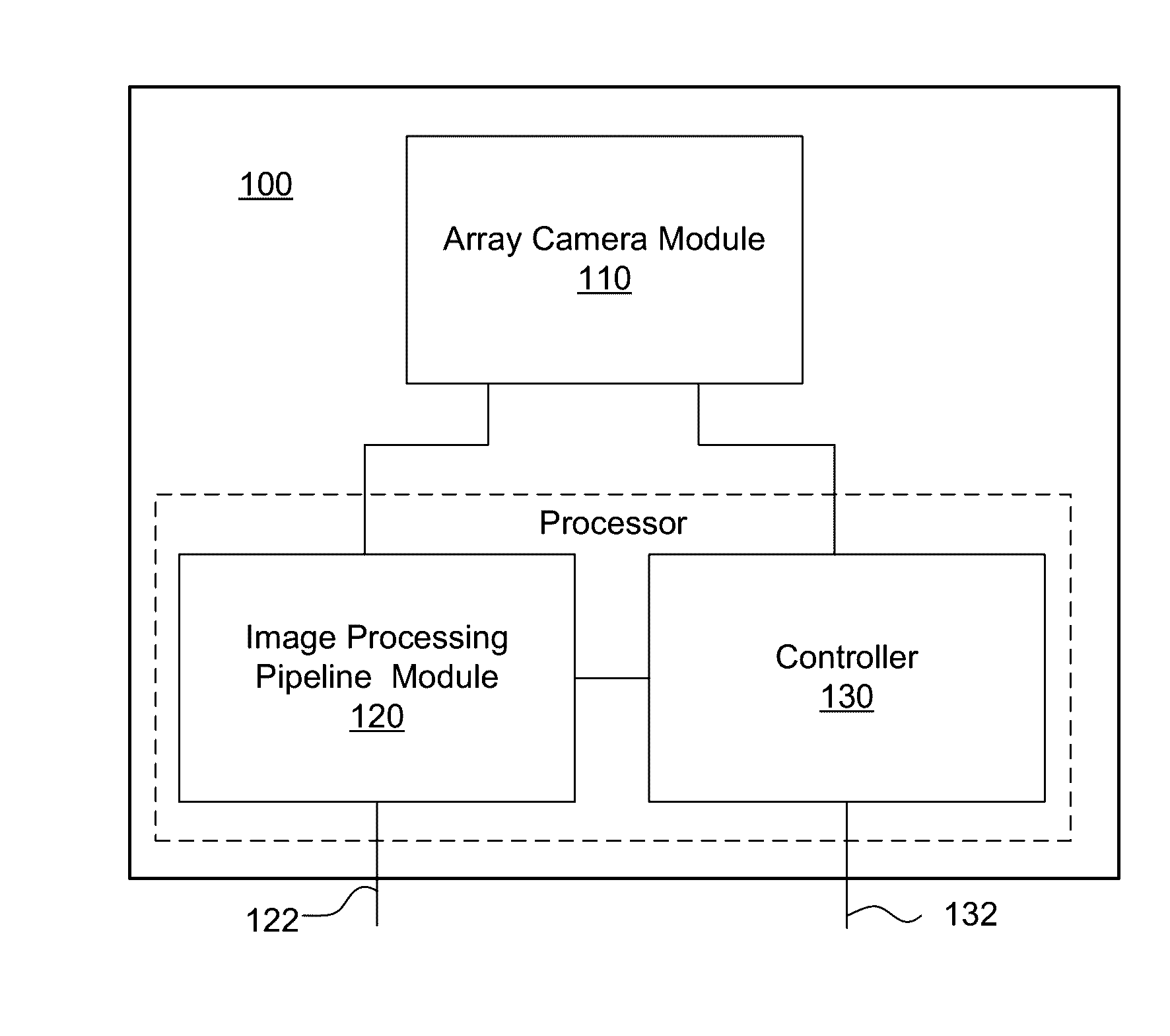
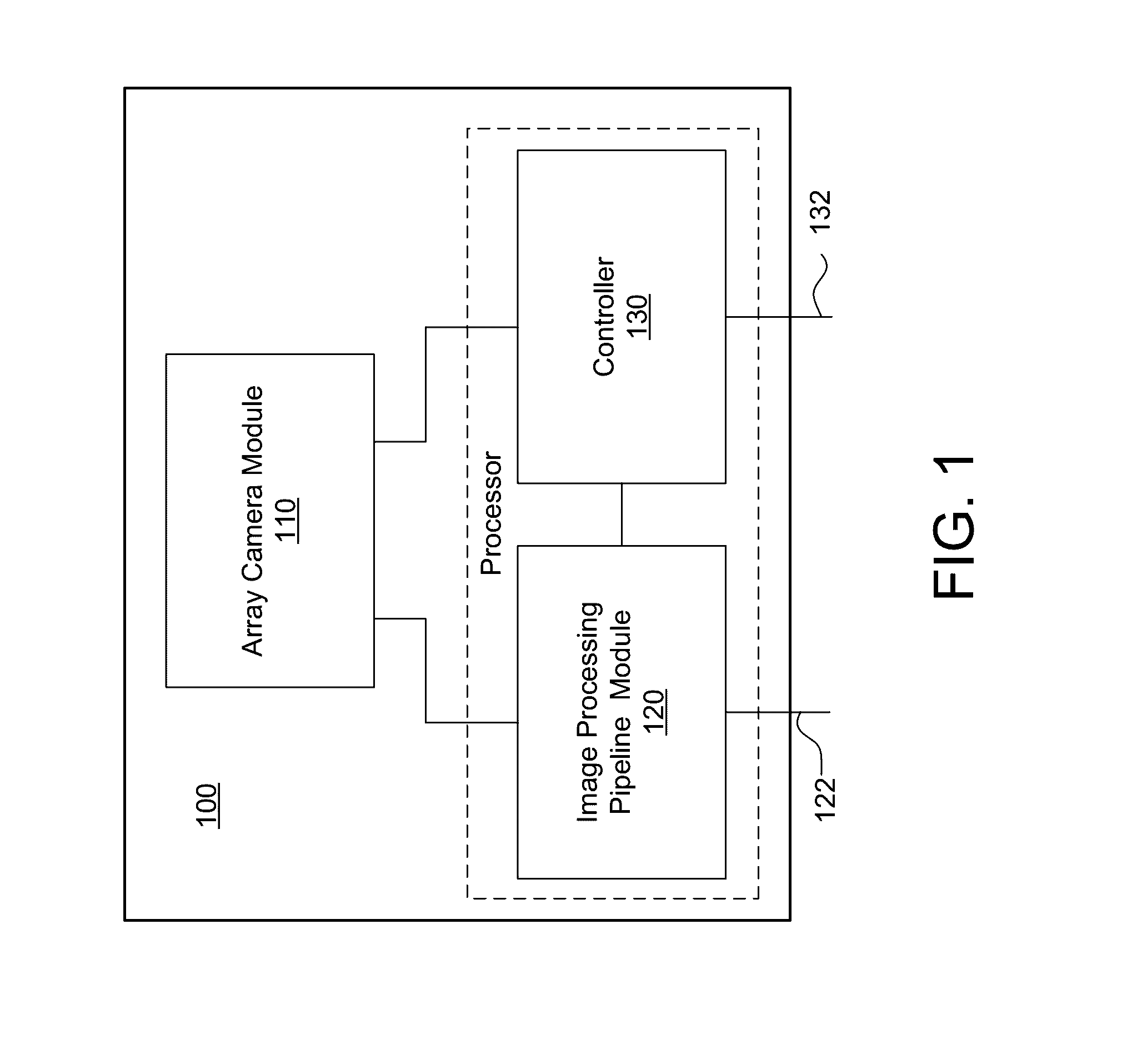
[0051]Turning now to the drawings, systems and methods for controlling the amount of aliasing in images captured by an array camera and for synthesizing higher resolution images from the captured images using super resolution (SR) processing in accordance with embodiments of the invention are illustrated. Images exhibit aliasing when they are sampled at too low a sampling frequency, resulting in visible steps on diagonal lines or edges (also referred to as “jaggies”) and artificial low frequency patterns (often referred to as Moiré). These artifacts are a product of the incorrect sampling of higher frequencies, which results in the higher frequencies folding back (being aliased) into lower frequencies. Aliasing is generally undesirable, however, array cameras in accordance with embodiments of the invention can utilize the high frequency information folded into the lower frequencies during SR processing, In a SR process, low resolution (LR) images that include sampling diversity (i.e...


PUM


Abstract

Imager arrays, array camera modules, and array cameras in accordance with embodiments of the invention utilize pixel apertures to control the amount of aliasing present in captured images of a scene. One embodiment includes a plurality of focal planes, control circuitry configured to control the capture of image information by the pixels within the focal planes, and sampling circuitry configured to convert pixel outputs into digital pixel data. In addition, the pixels in the plurality of focal planes include a pixel stack including a microlens and an active area, where light incident on the surface of the microlens is focused onto the active area by the microlens and the active area samples the incident light to capture image information, and the pixel stack defines a pixel area and includes a pixel aperture, where the size of the pixel apertures is smaller than the pixel area.

Description

CROSS-REFERENCES TO RELATED APPLICATIONS[0001]This application is a continuation of U.S. patent application Ser. No. 14 / 102,493 filed Dec. 10, 2013, which claimed priority under 35 USC 111(a) to PCT Patent Application No. PCT / US2012 / 056151, entitled “Systems and Methods for Controlling Aliasing in Images Captured by an Array Camera for Use in Super Resolution Processing”, filed Sep. 19, 2012, which claims priority to U.S. Provisional Patent Application No. 61 / 536,500, entitled “Aliasing Enhanced Super Resolution Processing Through Use of Pixel Apertures”, filed Sep. 19, 2011, the disclosures of which are incorporated herein by reference in their entirety.FIELD OF THE INVENTION[0002]The present invention relates to super resolution processing and more specifically to controlling aliasing during super resolution processing through use of pixel apertures.BACKGROUND[0003]In a typical imaging device, light enters through an opening (aperture) at one end of the imaging device and is direc...

Claims


Application Information

Patent Timeline
Patent Type & Authority Applications(United States)
IPC IPC(8): H04N5/232H04N5/225H04N13/02H04N9/097H04N13/232
CPCH04N5/23232H04N9/097H04N2013/0081H04N13/0271H04N5/2258H04N13/232H04N13/271H04N23/45H04N25/41H04N23/951H04N23/16
Inventor NAYAR, SHREEVENKATARAMAN, KARTIKPAIN, BEDABRATALELESCU, DAN
Owner PELICAN IMAGING CORP
Learn More