Light emitting device with phosphor layer
a technology of light emitting devices and phosphor layers, which is applied in the direction of semiconductor devices, basic electric elements, electrical appliances, etc., can solve the problems of reducing the benefit of the difficulty of making a light emitting device into a point light source, and achieves good light extraction efficiency, and increase reflectivity
- Summary
- Abstract
- Description
- Claims
- Application Information
AI Technical Summary
Benefits of technology
Problems solved by technology
Method used
Image
Examples
embodiment 1
[0029]Light Emitting Device
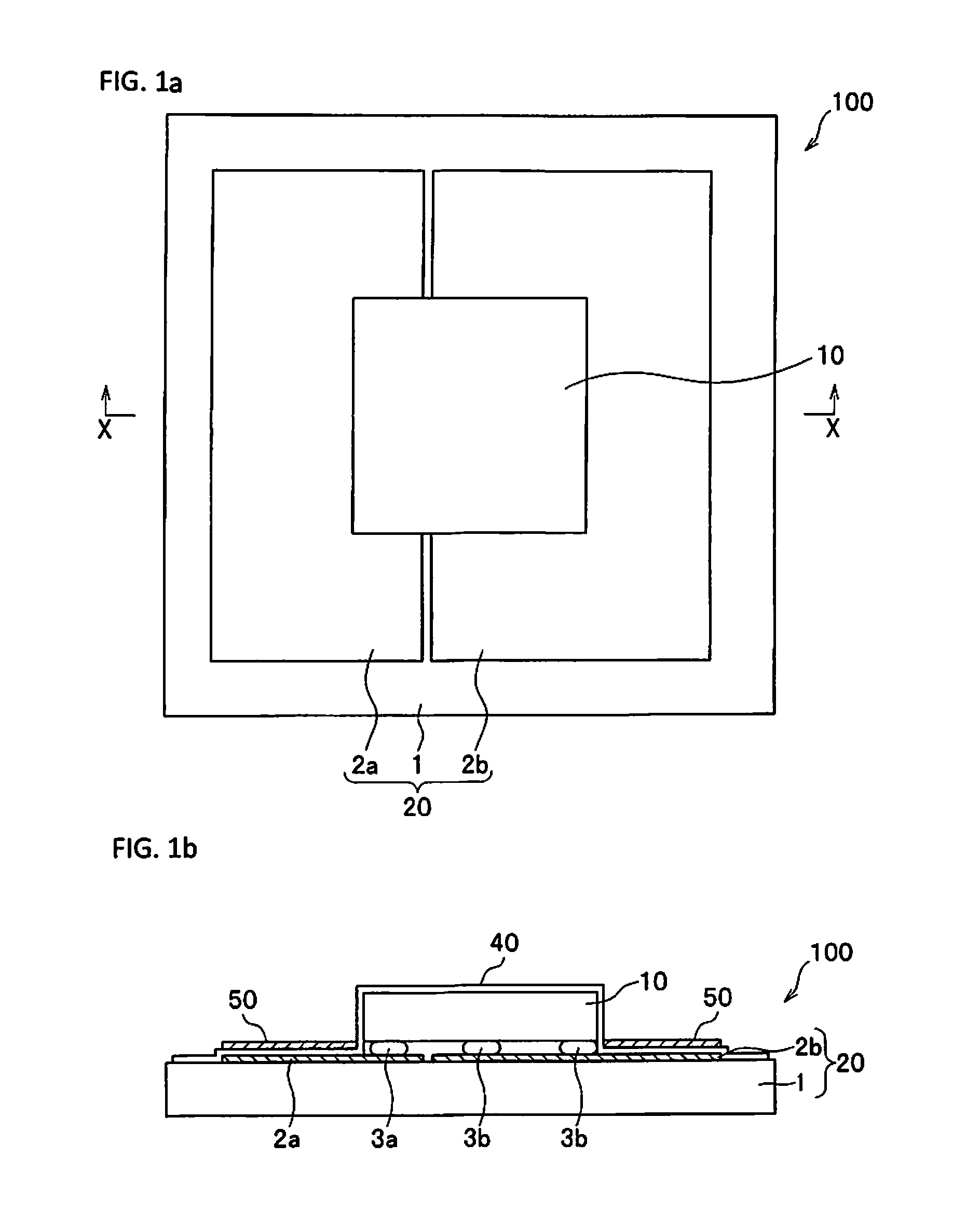
[0030]As shown in FIGS. 1a and 1b, a light emitting device 100 here mainly includes a base 1, conductive members 2a, 2b provided on the base 1, bumps 3a and 3b provided on the conductive members 2a, 2b, a light emitting element 10 provided on the bumps 3a and 3b, a phosphor layer 40 provided to the surface of the light emitting element 10 and the surface of a board (mounting board) 20, and a cover layer 50 that covers the phosphor layer 40 on the mounting board 20. The mounting board 20 here has the base 1 and the conductive members 2a, 2b. In order to facilitate an understanding of the configuration of the light emitting device of the present embodiment, the phosphor layer 40 and the cover layer 50 shown in FIG. 1b are not shown in FIG. 1a.
[0031]Mounting Board
[0032]As shown in FIGS. 1a and 1b, the mounting board 20 is a board on which the light emitting element 10 and other such electronic parts are mounted, and here includes the base 1 and the conductiv...
embodiment 2
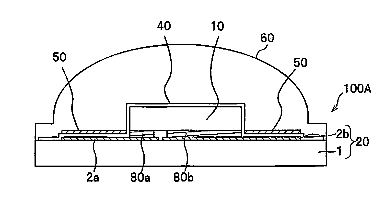
[0098]As shown in FIG. 3, a light emitting device 100A is such that the conductive members 2a, 2b and the light emitting element 10 are joined by joining members 80a and 80b.
[0099]With the light emitting device 100 discussed above, the light emitting element 10 is placed on the conductive members 2a, 2b with the bumps 3a and 3b in between them. As shown in FIG. 3, however, the joining members 80a and 80b can be used to place the light emitting element 10 on the conductive members 2a, 2b by eutectic bonding or resin bonding.
[0100]Examples of the material used in eutectic bonding include alloys whose main components are gold and tin, alloys whose main components are gold and silicon, and alloys whose main components are gold and germanium. Of these, AuSn is particular preferable. The material used for resin bonding can be a resin containing a conductive material.
embodiment 3
[0101]As shown in FIGS. 4a and 4b, a light emitting device 100B has a mounting portion A on which the board (mounting board) 20 is mounted, and a groove G formed surrounding the outer periphery of the mounting portion A. The mounting board 20 here is made of the base 1 (1a, 1b, and 1c) and conductive members 2a, 2b, and 2c. The phosphor layer 40 and the cover layer 50 that are shown in FIG. 4b are not shown in FIG. 4a in order to make the configuration of the present embodiment easier to understand. The phrase “the outer periphery of the mounting portion A” here refers to an area near the light emitting element 10, which surrounds the four sides of the light emitting element 10 on the board 20, in a plan view. Also, in this embodiment, the base 1c are also located around the outer periphery of the light emitting element 10, and are included in the concept of “near the light emitting element 10.”
[0102]The light emitting device 100B thus has the groove G formed in the mounting board 2...
PUM
 Abstract
Description
Claims
Application Information
 - R&D
- Intellectual Property
- Life Sciences
- Materials
- Tech Scout
- Unparalleled Data Quality
- Higher Quality Content
- 60% Fewer Hallucinations
Browse by: Latest US Patents, China's latest patents, Technical Efficacy Thesaurus, Application Domain, Technology Topic, Popular Technical Reports.
© 2025 PatSnap. All rights reserved.Legal|Privacy policy|Modern Slavery Act Transparency Statement|Sitemap|About US| Contact US: help@patsnap.com


