Semiconductor device

Active Publication Date: 2016-02-18
RENESAS ELECTRONICS CORP
View PDF0 Cites 0 Cited by
  • Summary
  • Abstract
  • Description
  • Claims
  • Application Information

AI Technical Summary

Benefits of technology

The present invention relates to a semiconductor device that includes a non-volatile memory and a dummy floating gate electrode. The problem addressed by the invention is the potential for erroneous determination as retention failure of a memory cell transistor due to the potential of the dummy floating gate electrode. The invention provides a solution by arranging the dummy floating gate electrode in a way that reduces the impact on the surrounding memory cell transistors and minimizes the potential for erroneous determination.

Problems solved by technology

A conventional semiconductor device including a non-volatile memory has been found to suffer the following problems.
Consequently, during baking in a subsequently conducted wafer test, movable ions in an interlayer insulating film are non-uniformly distributed due to a potential of the dummy floating gate electrode, and it has been found that the problem of erroneous determination as retention failure of a memory cell transistor in the memory cell array region, in particular in the vicinity of the gate contact region occurs.

Method used


Image

  • Semiconductor device
  • Semiconductor device
  • Semiconductor device

Examples


first embodiment

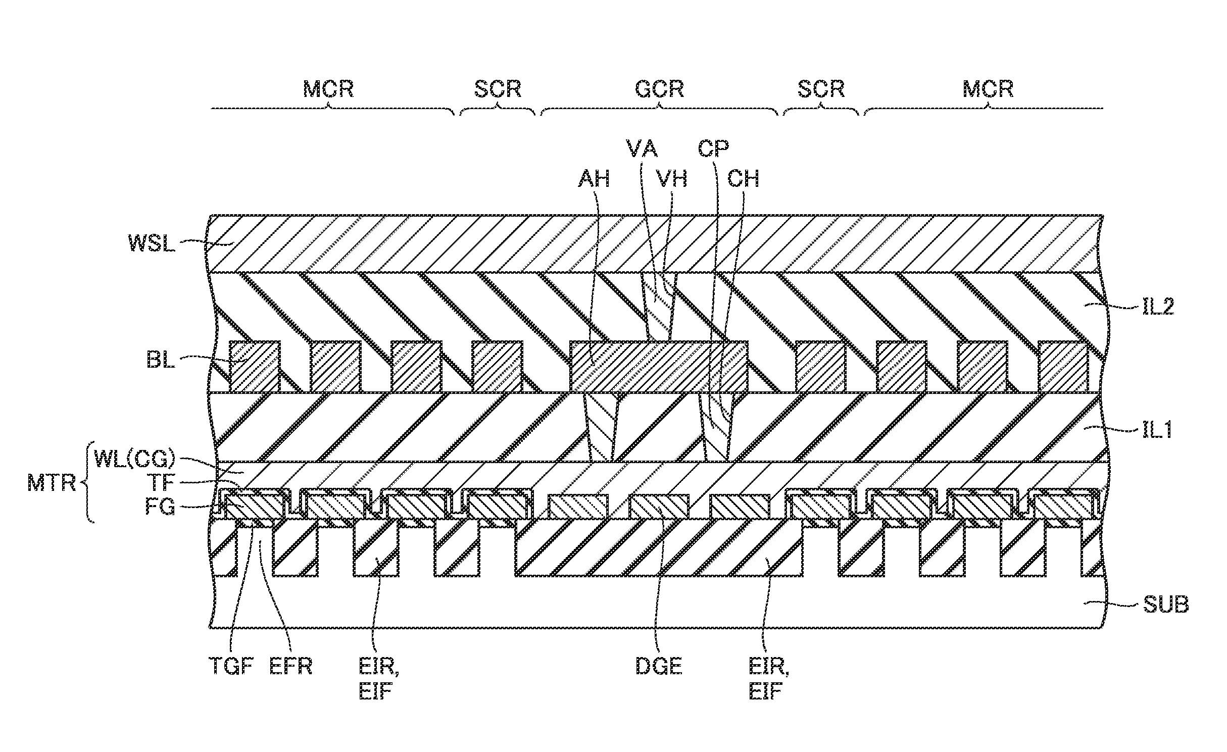
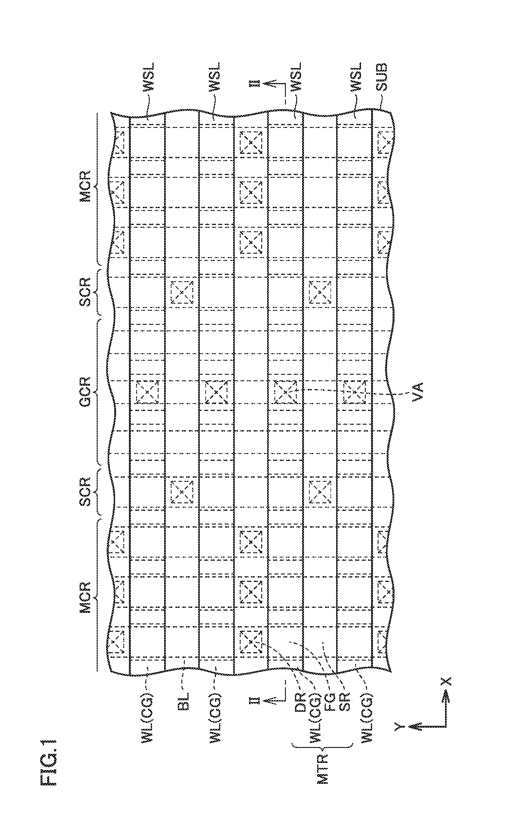
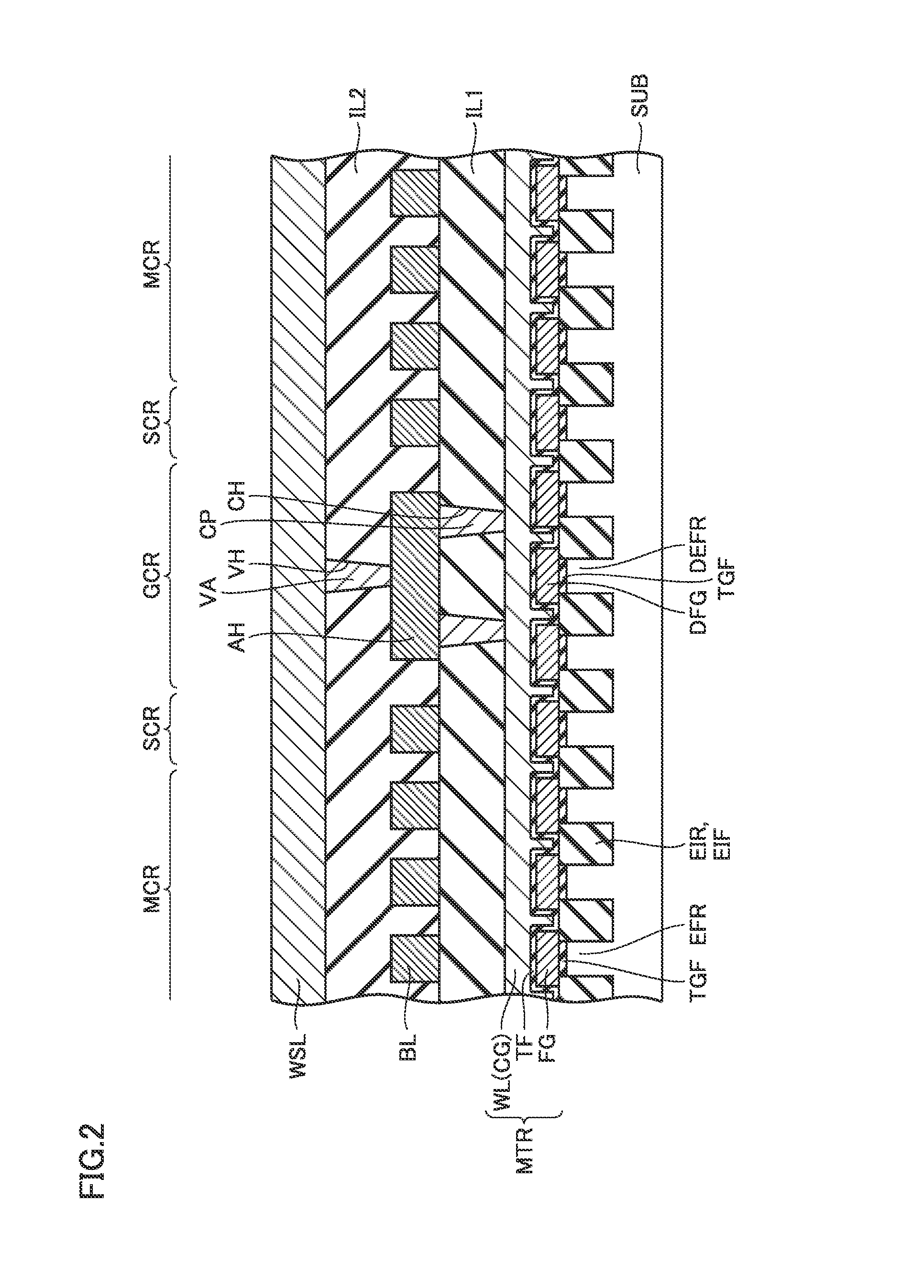
[0072]A first example of a semiconductor device including a non-volatile memory will be described here.

[0073]As shown in FIGS. 1 and 2, in a surface of a semiconductor substrate SUB, a memory cell array region MCR and a source contact region SCR (a first region) as well as a gate contact region GCR (a second region) are defined. In memory cell array region MCR and source contact region SCR, an element formation region EFR is defined by an element isolation region EIR. In gate contact region GCR, with a pattern in conformity with a pattern of element isolation region EIR formed in memory cell array region MCR, element isolation region EIR is formed and a dummy element formation region DEFR is defined.

[0074]In memory cell array region MCR and source contact region SCR, a floating gate electrode FG is formed on a prescribed portion in element formation region EFR, with a tunnel insulating film TGF being interposed. In gate contact region GCR, a dummy floating gate electrode DFG is form...

second embodiment

[0140]A second example of a semiconductor device including a non-volatile memory will now be described.

[0141]As shown in FIGS. 41, 42, and 43, in a surface of semiconductor substrate SUB, memory cell array region MCR and source contact region SCR as well as gate contact region GCR are defined. In memory cell array region MCR and source contact region SCR, element isolation region EIR defines element formation region EFR. In gate contact region GCR, element isolation region EIR is formed over the entire gate contact region GCR.

[0142]In memory cell array region MCR, memory cell transistor MTR is formed. In gate contact region GCR, dummy gate electrode DGE is formed. First interlayer insulating film IL1 formed from an undoped oxide film is formed to cover memory cell transistor MTR. In a portion of first interlayer insulating film IL1 located in gate contact region GCR, contact hole CH penetrating first interlayer insulating film IL1 and word line WL and reaching element isolation regi...

third embodiment

[0153]A third example of a semiconductor device including a non-volatile memory will now be described.

[0154]As shown in FIGS. 53 and 54, memory cell array region MCR and source contact region SCR as well as gate contact region GCR are defined in the surface of semiconductor substrate SUB. In memory cell array region MCR and source contact region SCR, element isolation region EIR defines element formation region EFR. In gate contact region GCR, element isolation region EIR is formed over the entire gate contact region GCR.

[0155]Memory cell transistor MTR is formed in memory cell array region MCR. Dummy gate electrode DGE is formed in gate contact region GCR. Dummy gate electrode DGE and word line WL (control gate electrode CG) are in direct contact with each other. First interlayer insulating film IL1 formed from an undoped oxide film is formed to cover memory cell transistor MTR. In a portion of first interlayer insulating film IL1 located in gate contact region GCR, contact hole CH...


PUM


Abstract

In a memory cell array region and a source contact region defined in a surface of a semiconductor substrate, a memory cell transistor including a floating gate electrode and a control gate electrode is formed. In a gate contact region, a dummy floating gate electrode is arranged to partially be superimposed on a dummy element formation region in a two-dimensional view. In a first interlayer insulating film and a second interlayer insulating film covering the memory cell transistor, a contact plug is formed to penetrate the first interlayer insulating film and a via is formed to penetrate a second interlayer insulating film.

Description

BACKGROUND OF THE INVENTION[0001]1. Field of the Invention[0002]The present invention relates to a semiconductor device and in particular it can suitably be used for a semiconductor device including a non-volatile memory including a floating gate electrode and a control gate electrode.[0003]2. Description of the Background Art[0004]A semiconductor device including a non-volatile memory having a floating gate electrode represents one of non-volatile memories. In a surface of a semiconductor substrate of such a semiconductor device, a memory cell array region and a gate contact region are defined. In the memory cell array region, a memory cell transistor is arranged. An interlayer insulating film is formed to cover the memory cell transistor. In a portion of the interlayer insulating film located in the gate contact region, a contact plug and a via for electrical connection between a control gate electrode and a word line shunt are formed.[0005]In the memory cell array region, a memor...

Claims


Application Information

Patent Timeline
IPC IPC(8): H01L27/115H01L23/522H01L23/535
CPCH01L27/11521H01L23/5226H01L23/535H01L2924/0002H01L29/40114H10B41/35H01L2924/00
Inventor ISHIGAKI, YOSHIYUKI
Owner RENESAS ELECTRONICS CORP
Why Eureka
Try Eureka