
Solder assembly temperature monitoring process

a technology of temperature monitoring and soldering, which is applied in the direction of heat measurement, instruments, soldering apparatus, etc., can solve the problems of significant scrap and/or rework expense, and the inability to achieve the desired electrical solder connection

Inactive Publication Date: 2016-01-14
IBM CORP
View PDF3 Cites 6 Cited by
  • Summary
  • Abstract
  • Description
  • Claims
  • Application Information

AI Technical Summary

Benefits of technology

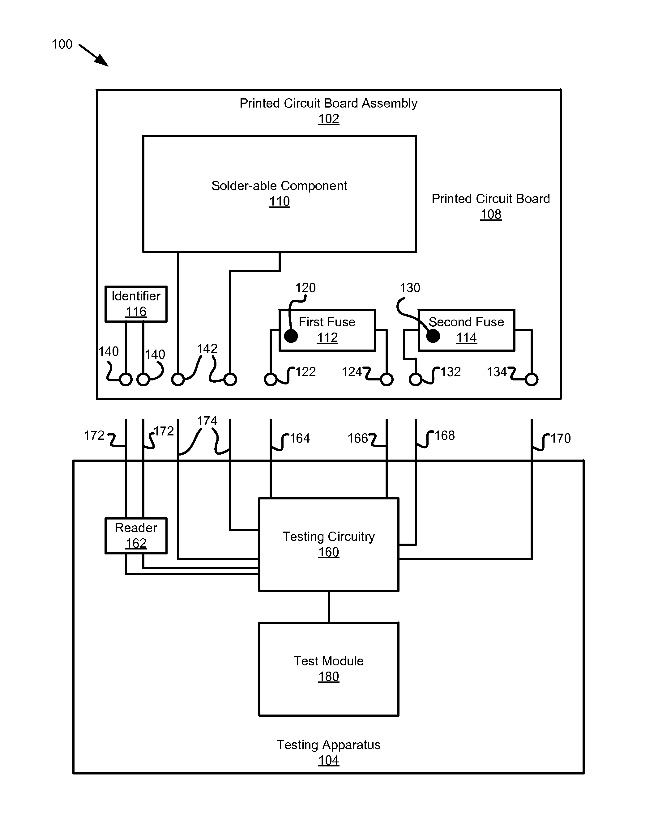
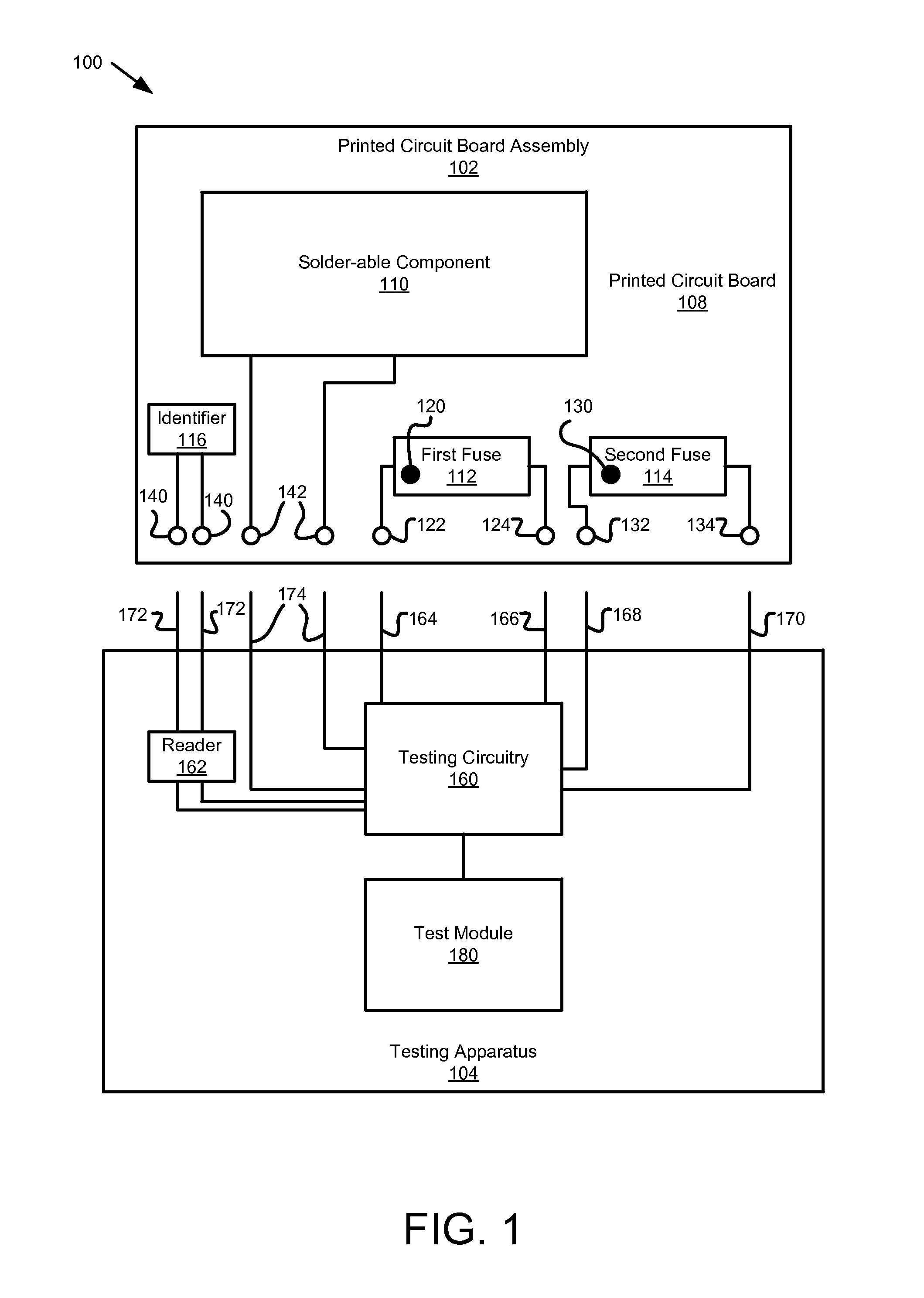
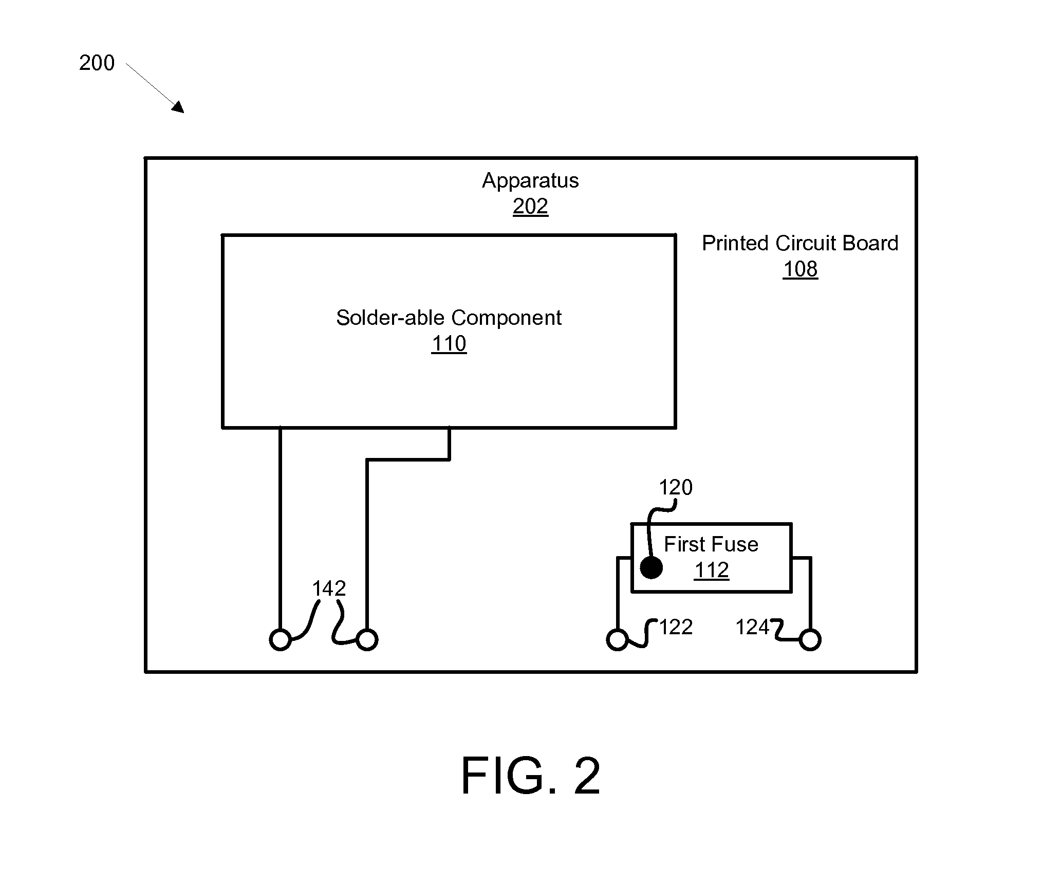
The patent describes a method for recording ambient temperatures during the manufacturing process of an integrated card assembly. A fuse is included in the assembly, which includes a printed circuit board and a solderable component. The fuse has a temperature-sensitive element that changes in response to exposure to ambient temperatures. The fuse is positioned on the printed circuit board and is connected to test conductors on the printed circuit board. The test conductors are connected to a testing apparatus, which includes probes and a test module to determine if the fuse has been exposed to temperatures that exceed the fuse's threshold temperature. The method allows for the recording of ambient temperatures during the manufacturing process and ensures the proper operation of the integrated card assembly.

Problems solved by technology

The solder assembly process should be carried out at a specific temperature profile for the printed circuit board assembly being manufactured; maximum oven temperatures that are too low or too high can cause the improper formation of the desired electrical solder connections.
If such a condition is not rapidly discovered during the manufacturing process, the result is significant scrap and / or rework expense as multiple bad boards are produced.

Method used


Image

  • Solder assembly temperature monitoring process
  • Solder assembly temperature monitoring process
  • Solder assembly temperature monitoring process

Examples


Embodiment Construction

[0027]Reference throughout this specification to “one embodiment,”“an embodiment,” or similar language means that a particular feature, structure, or characteristic described in connection with the embodiment is included in at least one embodiment. Thus, appearances of the phrases “in one embodiment,”“in an embodiment,” and similar language throughout this specification may, but do not necessarily, all refer to the same embodiment, but mean“one or more but not all embodiments” unless expressly specified otherwise. The terms “including,”“comprising,”“having,” and variations thereof mean “including but not limited to” unless expressly specified otherwise. An enumerated listing of items does not imply that any or all of the items are mutually exclusive and / or mutually inclusive, unless expressly specified otherwise. The terms “a,”“an,” and “the” also refer to “one or more” unless expressly specified otherwise.

[0028]Furthermore, the described features, advantages, and characteristics of...


PUM


Abstract

A method includes providing a printed circuit board (“PCB”) supporting a solderable component, and supporting a first fuse on the PCB, where the first fuse includes a first temperature-sensitive element that measurably changes in response to exposure to ambient thermal conditions exceeding a first threshold temperature. The PCB, the solderable component, and the first fuse define an apparatus. The method includes performing a PCB assembly manufacturing process, and then testing the first fuse to determine whether, during the PCB assembly manufacturing process, the first fuse was exposed to ambient thermal conditions exceeding a first threshold temperature. The first threshold temperature is a minimum temperature where the PCB assembly manufacturing process is to be carried out, a maximum temperature at which the PCB assembly manufacturing process is to occur, or a first intermediate temperature between the minimum and maximum temperatures.

Description

FIELD[0001]The subject matter disclosed herein relates to printed circuit board assemblies, and more particularly relates to methods for recording the temperatures encountered by a printed circuit board assembly during manufacturing and storage.BACKGROUNDDescription of the Related Art[0002]Many steps are used to form printed circuit board assemblies. Some of these steps require elevation of the printed circuit board assembly to certain temperatures. Specifically, a solder assembly process may be used to provide and / or connect conductive elements on the printed circuit board assembly by heating a conductive metal to a melted or liquidus temperature. The solder assembly process may be carried out in solder melting equipment such as a convection oven, vapor phase oven, or the like. The solder assembly process should be carried out at a specific temperature profile for the printed circuit board assembly being manufactured; maximum oven temperatures that are too low or too high can cause...

Claims


Application Information

Patent Timeline
Patent Type & Authority Applications(United States)
IPC IPC(8): G01K13/00H05K3/34
CPCG01K13/00H05K2203/162H05K2203/04H05K3/34B23K1/0016B23K1/008B23K1/015H05K13/082H05K13/083H05K13/0465G01K3/005
Inventor HUGO, STEPHEN MICHAELKELLY, MATTHEW STEPHEN
Owner IBM CORP
Learn More