
3D NAND array architecture

Active Publication Date: 2016-01-07
MACRONIX INT CO LTD
View PDF1 Cites 9 Cited by
  • Summary
  • Abstract
  • Description
  • Claims
  • Application Information

AI Technical Summary

Benefits of technology

The invention provides a way to understand some aspects of a new technology. The summary is not meant to identify important parts of the technology or what it is about. The purpose of the invention is to explain it in a simple way before moving on to the more detailed description. The technical effects of the invention are described in the claims, specification, and drawings.

Problems solved by technology

While 3D stacking memory structures hold the promise of greatly increased memory density, they also introduce significant process challenges because, among other things, of the need to etch very deep holes through many layers.
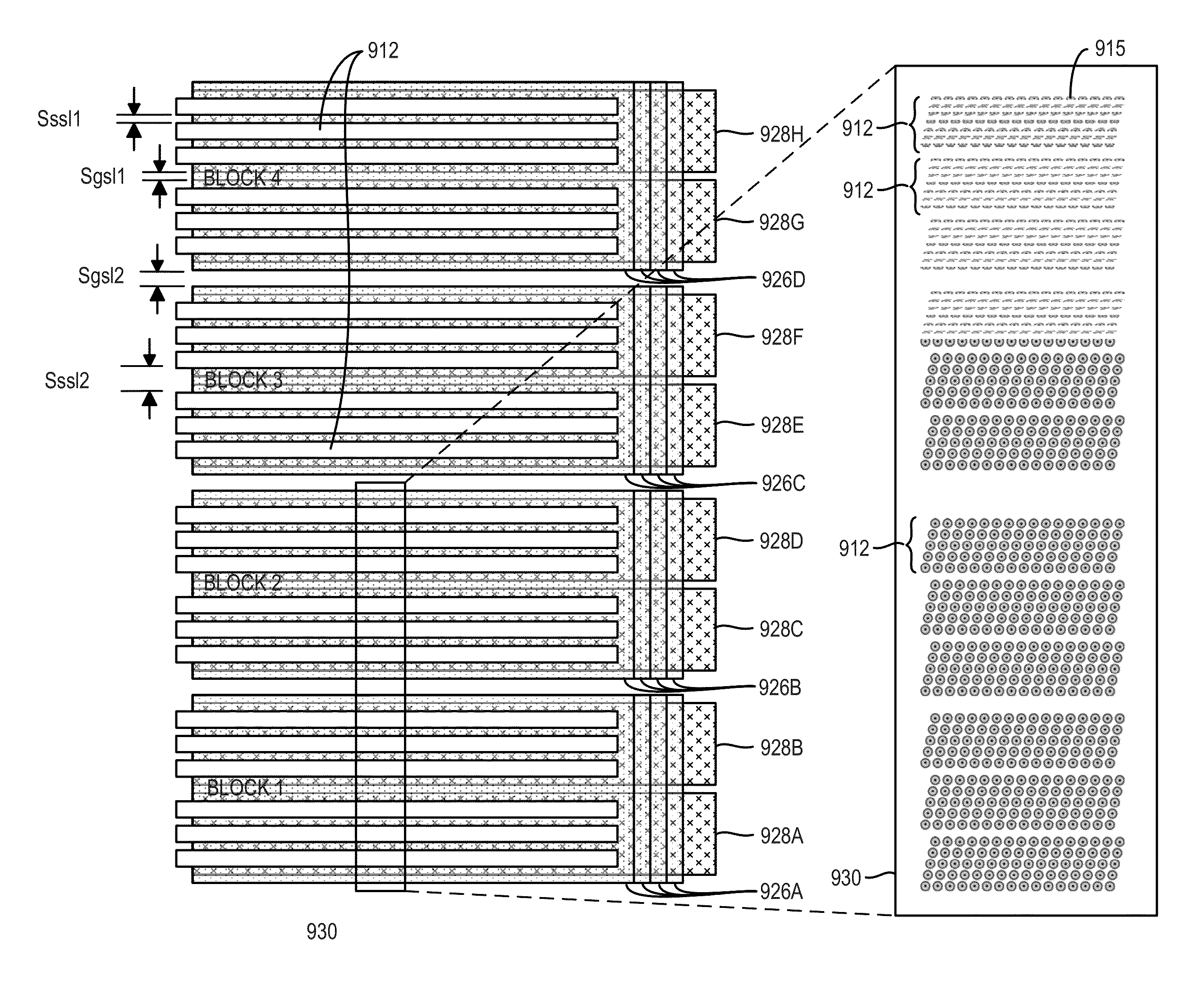
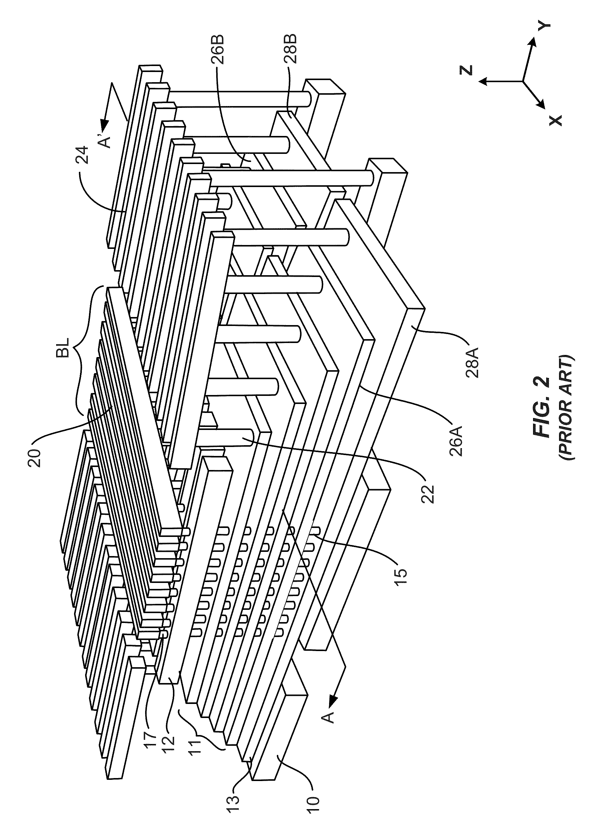
Unit cell capacitance also increases with the number of SSLs 12, thereby increasing power consumption and slowing device operation.
Thus increasing the number of memory layers also increases the number of SSLs 12, and again increases power consumption and slows device operation.

Method used


Image

  • 3D NAND array architecture
  • 3D NAND array architecture
  • 3D NAND array architecture

Examples


Embodiment Construction

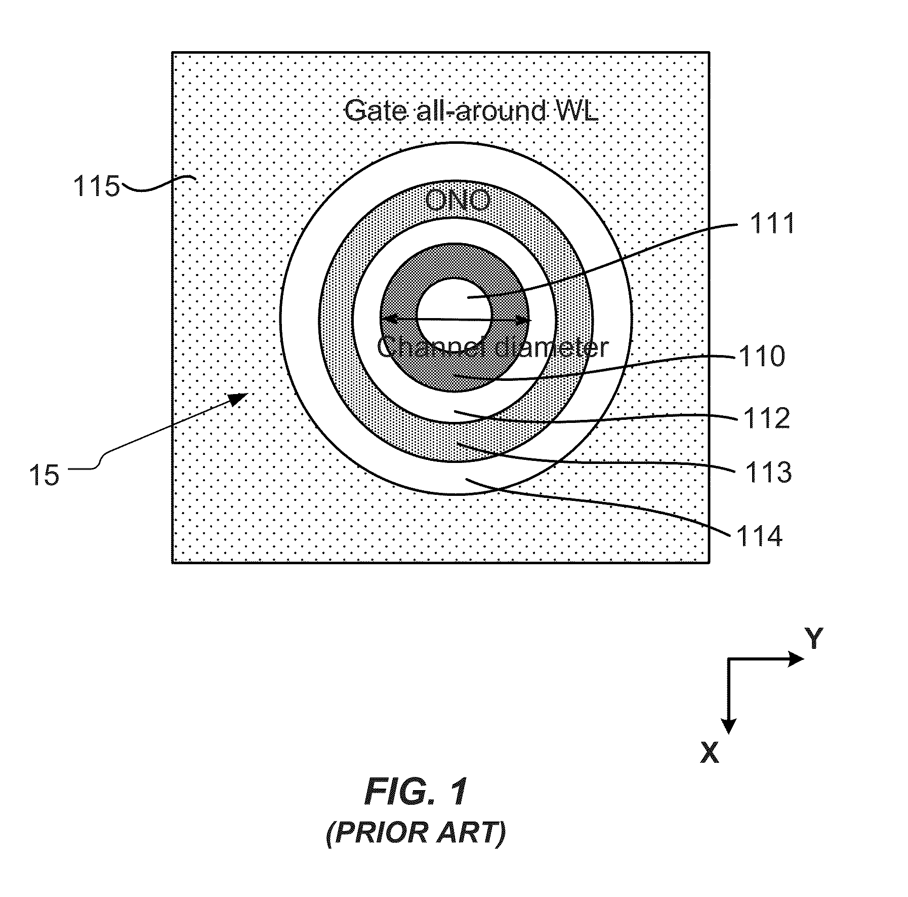
[0030]One solution to the problem of increasing bit density of 3D memory structures while reducing the negative impacts that such increases tend to cause, was discussed in the above-incorporated TWISTED ARRAY patent application. As described in more detail therein, in a memory device having a multilevel stack of conductive layers oriented parallel to a substrate, pillars oriented orthogonally to the substrate each include series-connected memory cells at cross-points between the pillars and the conductive layers. String select lines (SSLs) are disposed above the conductive layers, each intersection of a pillar and an SSL defining a respective select gate of the pillar. Bit lines are disposed above the string select lines. The pillars in the plurality of pillars are arranged on a regular grid which is rotated relative to the bit line conductors. The grid may have a square, rectangle or diamond-shaped unit cell, and may be rotated relative to the bit lines by an angle θ where tan(θ)=±...


PUM


Abstract

Roughly described, a memory device has a multilevel stack of conductive layers which are divided laterally into word lines. Vertically oriented pillars each include series-connected memory cells at cross-points between the pillars and the layers. String select lines run above the conductive layers and define select gates of the pillars. Bit lines run above the SSLs. The pillars are arranged on a regular grid having a unit cell area α, and adjacent ones of the string select lines have respective widths in the bit line direction which are at least as large as (α / pBL). Ground select lines run below the conductive layers and define ground select gates of the pillars. The ground select lines, too, may have respective widths in the bit line direction which are at least as large as (α / pBL).

Description

CROSS-REFERENCE TO OTHER APPLICATIONS[0001]This application is a Continuation-In-Part of each of the following U.S. patent applications, all incorporated by reference herein:[0002]U.S. application Ser. No. 14 / 157,550, filed 17 Jan. 2014, entitled THREE-DIMENSIONAL SEMICONDUCTOR DEVICE (P1020208), incorporated by reference herein.[0003]U.S. application Ser. No. 14 / 582,848, filed 24 Dec. 2014, entitled PARALLELOGRAM CELL DESIGN FOR HIGH SPEED VERTICAL CHANNEL 3D NAND MEMORY, by inventor Shih-Hung Chen (P1030091US, docket No. MXIC 2131-1), which is a Continuation-In-Part of the above-incorporated U.S. application Ser. No. 14 / 157,550, filed 17 Jan. 2014, entitled THREE-DIMENSIONAL SEMICONDUCTOR DEVICE (P1020208);[0004]U.S. application Ser. No. 14 / 582,963, filed 24 Dec. 2014, entitled TWISTED ARRAY DESIGN FOR HIGH SPEED VERTICAL CHANNEL 3D NAND MEMORY, by inventor Shih-Hung Chen (P1030081US, Docket No. MXIC 2132-1), which is also a Continuation-In-Part of the above-incorporated U.S. appl...

Claims


Application Information

Patent Timeline
IPC IPC(8): H01L27/115
CPCH01L27/11582H01L27/1157H01L27/0207H10B43/10H10B43/35H10B43/27
Inventor CHEN, SHIH-HUNG
Owner MACRONIX INT CO LTD
Learn More