Semiconductor device
- Summary
- Abstract
- Description
- Claims
- Application Information
AI Technical Summary
Benefits of technology
Problems solved by technology
Method used
Image
Examples
example 1
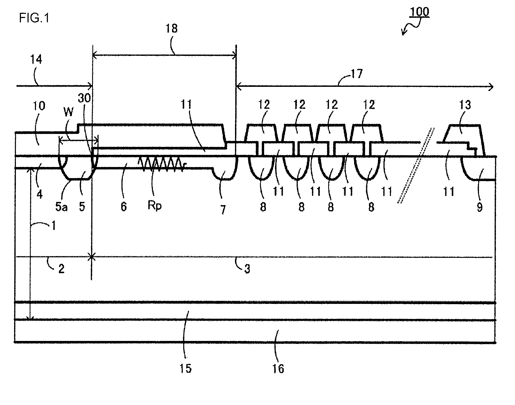
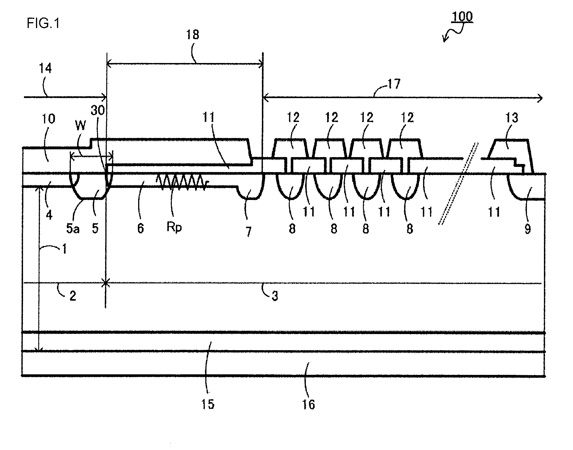
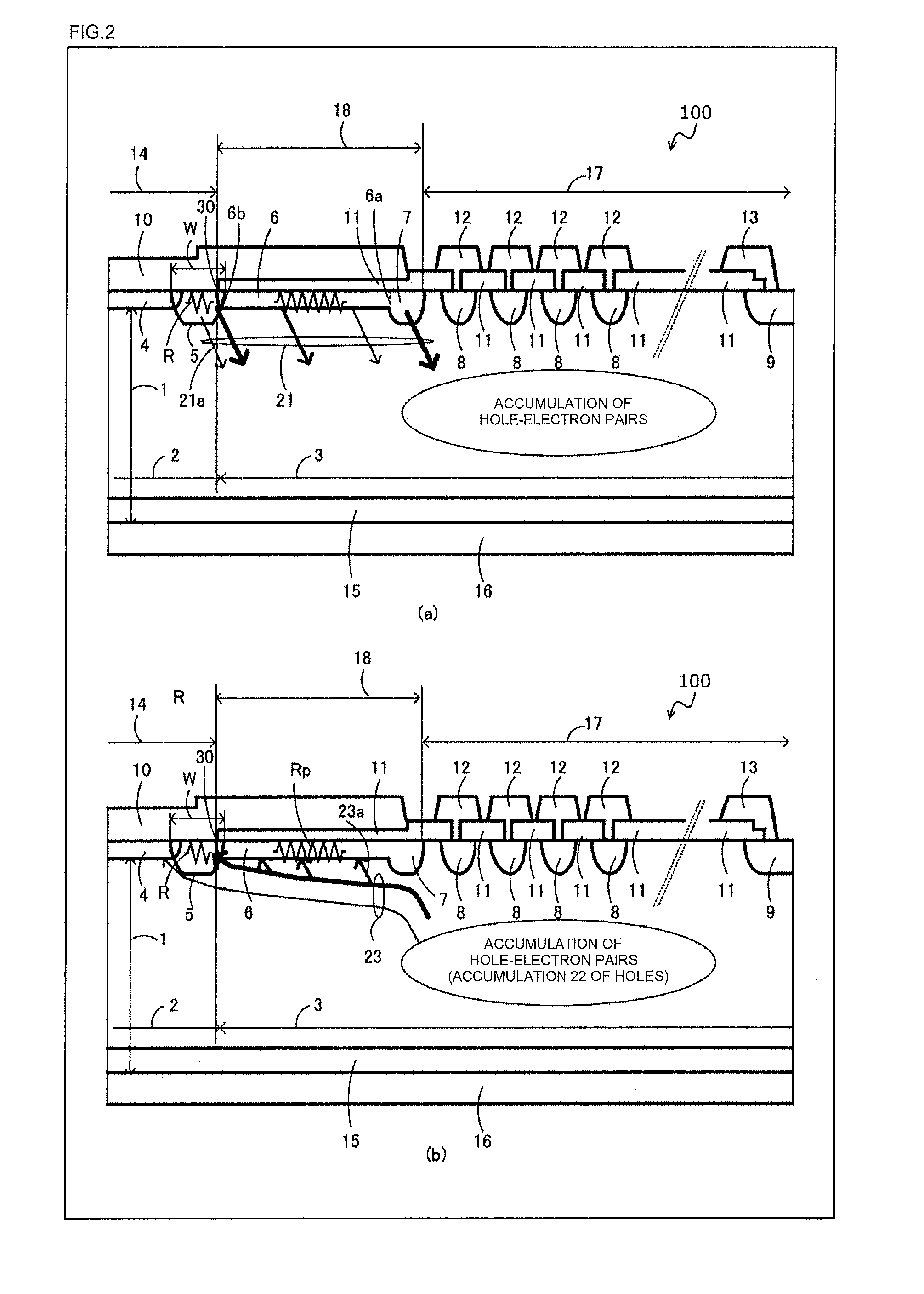
[0066]FIG. 1 is a substantial part cross-sectional view of a semiconductor device 100 according to Example 1 of the present invention. FIG. 1 illustrates a substantial part cross section of an FWD corresponding to an FWD 88 of FIG. 8, specifically the substantial part cross section of the semiconductor device from the vicinity thereof of an active part edge part through an outer circumferential part of the semiconductor substrate. In FIG. 1, the semiconductor device 100 is provided with a p-anode region 4 (an example of a first semiconductor region of a second conductive type) disposed on an upper surface of an n-drift region 2 (an example of a semiconductor substrate of a first conductive type). On the n-drift region 2, a p-diffusion region 5 (an example of one of the diffusion regions of the second conductive type) is provided which is disposed so as to be in contact with the p-anode region 4 and has a lower density and a deeper diffusion depth than the p-anode region 4. In an n−-...
example 2
[0087]FIG. 3 is a substantial part cross-sectional view of a semiconductor device 200 according to Example 2 of the present invention. A difference relative to Example 1 exists in that a high-density p-region 25 (p+) whose diffusion depth is shallow is formed on the p-diffusion region 5 and the p-anode region 4. When a surface density of the p-diffusion region 5 is low, an ohmic contact to the anode electrode 10 becomes difficult, so that a contact resistance becomes increased. When the contact resistance becomes increased, an amount of the withdrawal holes from the p-diffusion region 5 is decreased, and thus the withdrawal of the holes occurs mostly in the p-anode region 4. Then, the electric current concentration occurs in the p-diffusion region 4, which leads to the element breakdown.
[0088]As a countermeasure to prevent this, it is preferable to provide the p-region 25 that has a higher impurity density and a shallower diffusion depth than the p-diffusion region 5, in order to de...
example 3
[0090]FIG. 4 is a substantial part cross-sectional view of a semiconductor device 300 according to Example 3 of the present invention. The semiconductor device 300 is different from Example 1 in the following two points. A first point is that a resistance region 26, having a deeper diffusion depth than the resistance region 6 and the p-anode region 4 and a shallower diffusion depth than the p-guard ring regions 8, is disposed so as to be in contact with the resistance edge part region 7 and the p-anode region 4. A second point is that an edge part of a location where the p-anode region 4 is in contact with the anode electrode 10 is kept away (receded) from the resistance region 26. In FIG. 4, the insulating film 11 is illustrated as a two-layer insulating film of the PSG film 11 b of a phosphorous glass and the thermal oxidation film 11a.
[0091]The buffer region 18 in Example 3 has the three different resistance regions. A first resistance region is the p-anode region 4 that extends...
PUM
 Abstract
Description
Claims
Application Information
 - Generate Ideas
- Intellectual Property
- Life Sciences
- Materials
- Tech Scout
- Unparalleled Data Quality
- Higher Quality Content
- 60% Fewer Hallucinations
Browse by: Latest US Patents, China's latest patents, Technical Efficacy Thesaurus, Application Domain, Technology Topic, Popular Technical Reports.
© 2025 PatSnap. All rights reserved.Legal|Privacy policy|Modern Slavery Act Transparency Statement|Sitemap|About US| Contact US: help@patsnap.com


