
Nitride semiconductor light-emitting device having excellent brightness and ESD protection properties

a technology of nitride and semiconductor, which is applied in the direction of semiconductor devices, basic electric elements, electrical appliances, etc., to achieve the effects of high brightness characteristics, increased probability of recombination of electrons and holes, and smooth movemen

Inactive Publication Date: 2015-09-17
HC SEMITEK CORP
View PDF2 Cites 14 Cited by
  • Summary
  • Abstract
  • Description
  • Claims
  • Application Information

AI Technical Summary

Benefits of technology

The nitride semiconductor light-emitting device has a high brightness and can increase the probability of recombination of electrons and holes by including an electron blocking layer with p-type impurity-doped AlInGaN that increases the concentration of indium as it moves away from the active layer. Additionally, the device has an excellent electrostatic discharge (ESD) protection effect based on the electron blocking layer's high current dispersion effect due to the addition of indium.

Problems solved by technology

The electron blocking layer formed of AlGaN has a high ability to block electrons, but has a problem in that it also acts as a hole barrier.

Method used


Image

  • Nitride semiconductor light-emitting device having excellent brightness and ESD protection properties
  • Nitride semiconductor light-emitting device having excellent brightness and ESD protection properties
  • Nitride semiconductor light-emitting device having excellent brightness and ESD protection properties

Examples


examples

[0047]Hereinafter, the construction and effect of the present invention will be descried in further detail with reference to preferred examples. It is to be understood, however, that these examples are for illustrative purposes only and are not intended to limit the scope of the present invention in any way. Contents not disclosed herein can be sufficiently understood by those skilled in the art, and thus the description thereof is omitted.

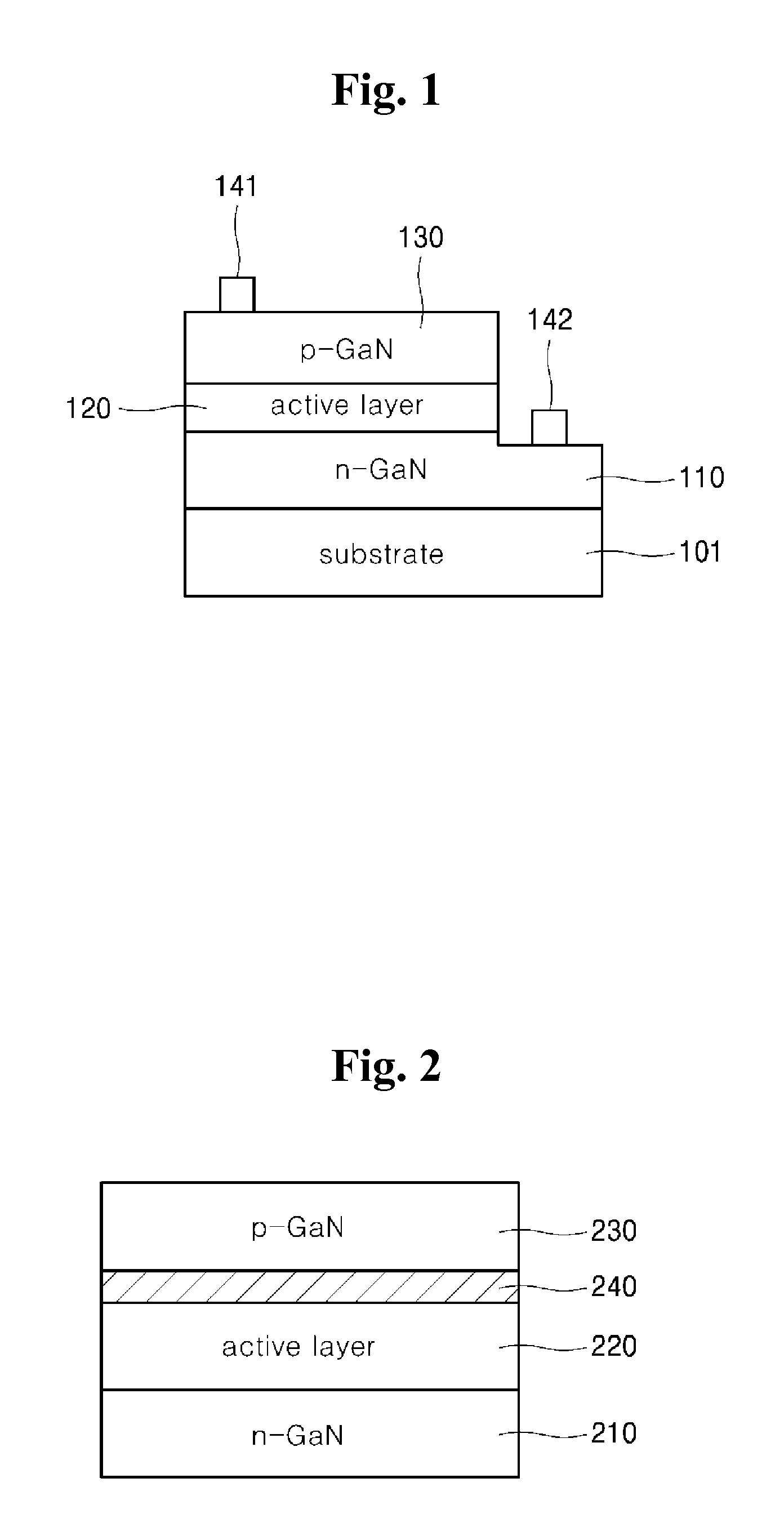
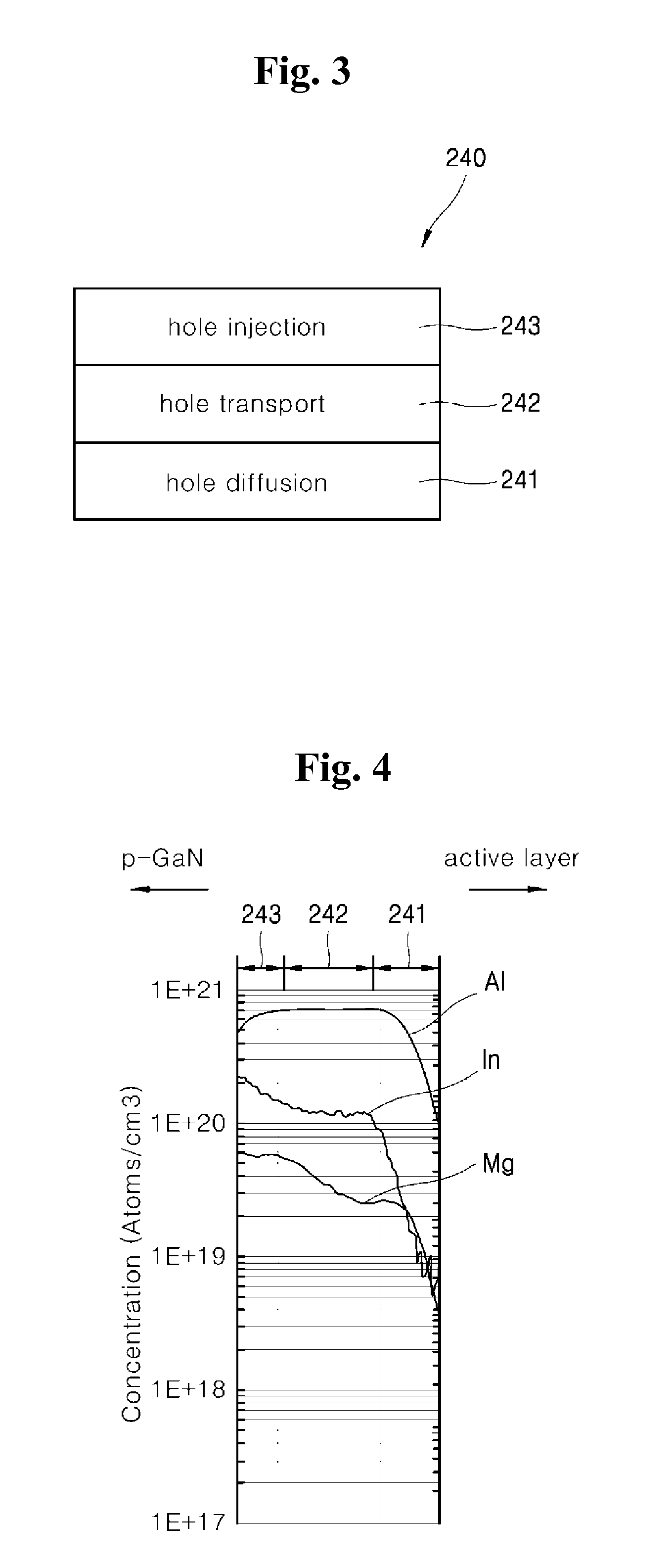
[0048]FIG. 4 shows the concentration profile of each of components contained in an electron blocking layer used in Example 1 of the present invention. As shown in FIG. 4, the electron blocking layer used in Example 1 was formed of AlInGaN, and the concentration of magnesium in the electron blocking layer showed a tendency to increase as the electron blocking layer moved away from the active layer.

[0049]FIG. 5 shows the concentration profile of each of components contained in an electron blocking layer used in Comparative Example 1. As shown in FIG...


PUM


Abstract

Disclosed is a nitride semiconductor light-emitting device having excellent brightness and ESD protection properties. The nitride semiconductor light-emitting device according to the present invention includes an electron blocking layer that is disposed between a p-type nitride semiconductor layer and an active layer, wherein said electron blocking layer includes AlInGaN, and the concentration of indium increases in the electron blocking layer as said layer progressively moves away from the active layer.

Description

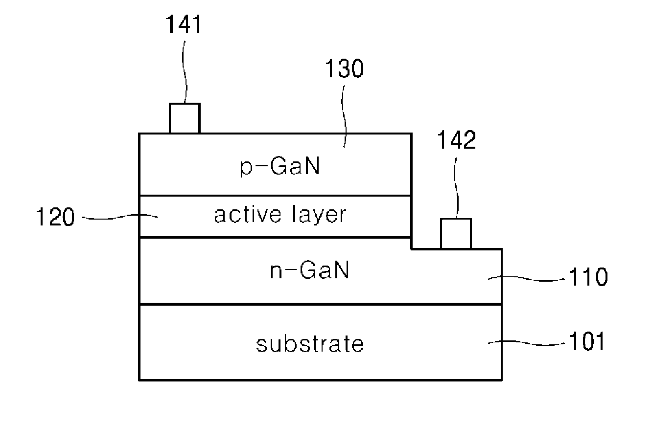
TECHNICAL FIELD[0001]The present invention relates to a nitride semiconductor light-emitting device, and more particularly, to a nitride semiconductor light-emitting device that can exhibit excellent brightness and electrostatic discharge (ESD) characteristics as a result of controlling the composition of an electron blocking layer (EBL) formed between an active layer and a p-type nitride semiconductor layer.BACKGROUND ART[0002]A light-emitting device is a device that emits light upon the recombination of electrons and holes.[0003]Typical light-emitting devices include a nitride semiconductor light-emitting device based on a nitride semiconductor represented by GaN. The nitride semiconductor light-emitting device has a high band gap, and thus can emit various colored lights. In addition, it has excellent thermal stability, and thus has been used in various fields.[0004]FIG. 1 shows a general nitride semiconductor light-emitting device.[0005]Referring to FIG. 1, the nitride semicondu...

Claims


Application Information

Patent Timeline
Patent Type & Authority Applications(United States)
IPC IPC(8): H01L33/14H01L33/32
CPCH01L33/325H01L33/145H01L33/04H01L33/14H01L33/025
Inventor LEE, WON-YONGPARK, JUNG-WONLEE, SUNG-HAKKWON, TAE-WANCHOI, WON-JIN
Owner HC SEMITEK CORP
Learn More